Semiconductor device and method for diagnosing semiconductor device

A diagnostic method and semiconductor technology, applied in semiconductor devices, semiconductor working life testing, single semiconductor device testing, etc., can solve problems such as aluminum wire degradation, and achieve the effect of high-precision degradation

Pending Publication Date: 2021-10-08
MITSUBISHI ELECTRIC CORP
View PDF1 Cites 0 Cited by
  • Summary
  • Abstract
  • Description
  • Claims
  • Application Information

AI Technical Summary

Problems solved by technology

[0003] Since there is a difference in the linear expansion coefficient of the silicon (Si) chip and that of the aluminum wire, the aluminum wire deteriorates due to repeated application of thermal stress

Method used


Image

  • Semiconductor device and method for diagnosing semiconductor device
  • Semiconductor device and method for diagnosing semiconductor device
  • Semiconductor device and method for diagnosing semiconductor device

Examples


no. 1 Embodiment approach

[0038] Next, the semiconductor device and the diagnostic method of the semiconductor device according to the present embodiment will be described.

[0039]

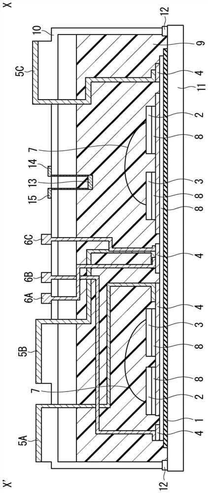
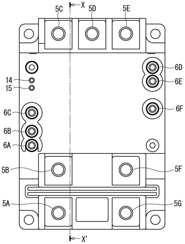
[0040] figure 1 It is a side view schematically showing an example of the structure of a semiconductor device (for example, a power module) according to this embodiment. exist figure 1 The encapsulation material 9 is described partially in perspective in the middle.

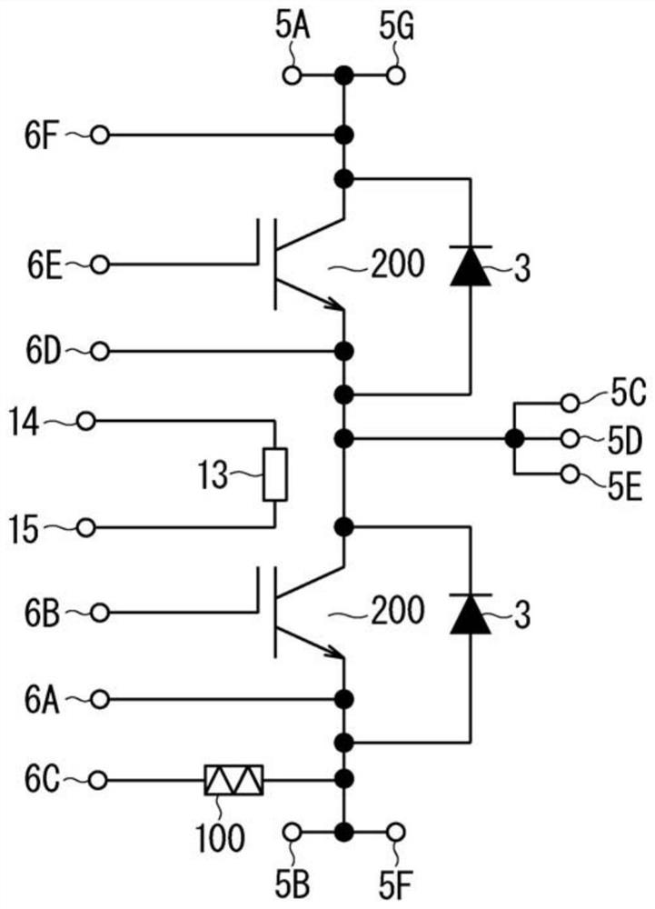
[0041] Such as figure 1 As illustrated in , the semiconductor device has: an insulating substrate 1 (or an insulating sheet); a conductive bonding material 8 formed on the upper surface of the insulating substrate 1; an electrode pattern 4 disposed on the upper surface of the conductive bonding material 8. The metal-oxide-semiconductor field-effect transistor (MOSFET) chip 2, which is a semiconductor element, is arranged on the electrode pattern 4 via a conductive bonding material 8. The upper surface; a Schottky barrier diode (Schottky barrier diode, ...

no. 2 Embodiment approach

[0064] The semiconductor device and the diagnostic method of the semiconductor device according to the present embodiment will be described. In addition, in the following description, the same constituent elements as those described in the above-described embodiments are denoted by the same reference numerals and shown in figures, and detailed descriptions thereof are appropriately omitted.

[0065]

[0066] Figure 4 It is a side view schematically showing an example of the structure of the semiconductor device according to this embodiment. exist Figure 4 The encapsulation material 9 is partially described in perspective in the middle.

[0067] Such as Figure 4 As exemplified in , the semiconductor device has an insulating substrate 1, a conductive bonding material 8, an electrode pattern 4, a MOSFET chip 2, an SBD chip 3, a metal wire 7, a base plate 11, an insert case 10, a main electrode terminal 5A, The main electrode terminal 5B and the main electrode terminal 5C...

no. 3 Embodiment approach

[0080] The semiconductor device and the diagnostic method of the semiconductor device according to the present embodiment will be described. In addition, in the following description, the same constituent elements as those described in the above-described embodiments are denoted by the same reference numerals and shown in figures, and detailed descriptions thereof are appropriately omitted.

[0081]

[0082] Figure 7 It is a side view schematically showing an example of the structure of the semiconductor device according to this embodiment. exist Figure 7 The encapsulation material 9 is described partially in perspective in the middle.

[0083] Such as Figure 7 As exemplified in , the semiconductor device has an insulating substrate 1, a conductive bonding material 8, an electrode pattern 4, a MOSFET chip 2, an SBD chip 3, a metal wire 7, a base plate 11, an insert case 10, a main electrode terminal 5A, The main electrode terminal 5B, the main electrode terminal 5C, t...


PUM


Abstract

Provided is a technique for enhancing the accuracy of deterioration diagnosis in a semiconductor device. The semiconductor device relating to the technique disclosed in the present specification is provided with: a case (10); semiconductor chips (2, 3) inside the case; a metal wire (7) joined to the upper surfaces of the semiconductor chips; at least one test piece (13 -13E) inside the case; and a pair of terminals (14 - 14E, 15 - 15E) provided outside the case and connected to the test piece. The test piece is separated from the metal wire (7) inside the case.

Description

technical field [0001] The technology disclosed in this specification relates to a semiconductor device and a diagnostic method for the semiconductor device. Background technique [0002] In a conventional power semiconductor device, a diagnosis of deterioration due to heat generation or a deterioration diagnosis of a power cycle life is performed using wire wiring inside the power semiconductor device. [0003] Since there is a difference in the linear expansion coefficient of the silicon (Si) chip and that of the aluminum wire, the aluminum wire is deteriorated due to repeated application of thermal stress. The above-mentioned deterioration diagnosis can be performed based on the cracks generated in the aluminum wiring due to the repeated thermal stress (for example, refer to Patent Document 1). [0004] Patent Document 1: Japanese Patent Laid-Open No. 2009-22084 Contents of the invention [0005] If the method of diagnosing deterioration using lead wires as described ...

Claims


Application Information

Patent Timeline
IPC IPC(8): H02M1/00G01R31/26H02M7/48
CPCH01L2224/48137H01L2224/32225H01L2924/3512H01L2924/13091H01L2924/12032H01L2924/13055H01L2924/10253H01L2924/10271H01L2924/1033H01L2224/45147H01L2224/45624H01L2224/45124H01L2224/29339H01L2224/83424H01L2224/83455H01L24/32H01L24/29H01L24/45H01L24/48H01L24/83H01L23/49811G01R31/2642G01R31/2644G01R31/2884H01L25/072H01L23/053H01L23/24H01L22/34H01L22/14H01L2924/00014H01L23/538H01L25/18H01L2224/4801H01L2924/10272H01L2924/2076H02M7/537
Inventor 北岛由美惠
Owner MITSUBISHI ELECTRIC CORP
Why Eureka
Try Eureka