Multilayer printed circuit board and method of making the same

A multi-layer printing and manufacturing method technology, applied in multi-layer circuit manufacturing, printed circuit manufacturing, printed circuit, etc., can solve problems such as multi-layer printed circuit boards are easy to warp, and achieve the elimination of local board internal stress and reduce board internal stress. Stress, the effect of reducing the difference in residual copper ratio

Active Publication Date: 2022-08-09
SHENZHEN KINWONG ELECTRONICS
View PDF11 Cites 0 Cited by
  • Summary
  • Abstract
  • Description
  • Claims
  • Application Information

AI Technical Summary

Problems solved by technology

[0003] The application provides a multi-layer printed circuit board and its manufacturing method to solve the problem that the multi-layer printed circuit board is easy to warp

Method used


Image

  • Multilayer printed circuit board and method of making the same
  • Multilayer printed circuit board and method of making the same
  • Multilayer printed circuit board and method of making the same

Examples


Embodiment Construction

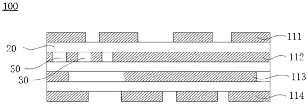
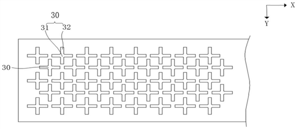
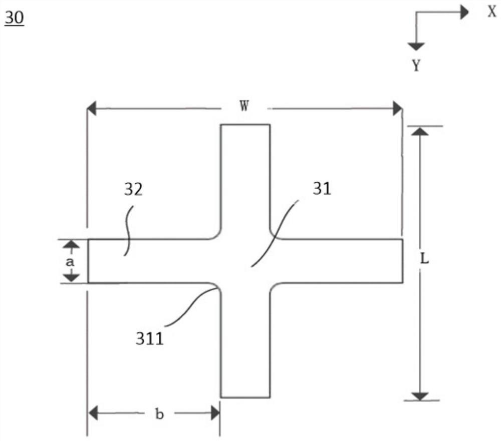
[0030] In order to make the purpose, technical solutions and advantages of the invention more clear and clear, the following combination of attached figures is an embodiment to further explain the present invention in detail. It should be understood that the specific embodiments described here are only used to explain the invention and do not limit the present invention.

[0031] It should be noted that when the part is called "fixed in" or "set in" another part, it can be directly or indirectly on the other component. When one part is called "connecting" another component, it can be directly or indirectly connected to the other component. The term "first" and "second" are only used to facilitate description of the purpose, not to be understood as the number of indications or implications or implicitly indicating the number of technical features. The meaning of "multiple" is more than two or two, unless there is another clear and specific limit.

[0032] It should also be noted th...


PUM


Abstract

The present application is applicable to the technical field of printed circuit boards, and proposes a multilayer printed circuit board, which includes at least two circuit layers, the at least two circuit layers include copper foil areas, and at least one layer of the circuit layers has a copper foil area. There are a plurality of copper digging parts arranged in an array, and the copper digging parts are formed by removing part of the copper foil. The present application also proposes a method for manufacturing a multilayer printed circuit board. The above-mentioned multilayer printed circuit board and the manufacturing method thereof can adjust the residual copper ratio of the circuit layer, eliminate local stress in the board, and further solve the problem of board warpage.

Description

Technical field [0001] The present invention involves a multi -layer printing line technology field, which specializes in a multi -layer printing line board and its production method. Background technique [0002] At present, the functions of electronic products such as mobile phones are increasing and the volume is getting thinner and thinner. Under this development trend, the printing line boards assembled in electronic products also require thinner and thinner. Now the 10 -layer high -density interconnection (HighDensity Interconnector (HDI) plate thickness is less than 0.6mm. Such HDI boards are prone to warning in production. Essence Among them, the copper area of ​​each layer in the printing line board is unevenly distributed. At the same time, the internal stress of the printing line board is the main reason for leading. At present, it is usually improving the problem of turning on the board through the method of pressing the finished product, but this method has not impro...

Claims


Application Information

Patent Timeline
Patent Type & Authority Patents(China)
IPC IPC(8): H05K1/14H05K3/46
CPCH05K3/4611H05K1/14
Inventor 肖安云陈前王俊
Owner SHENZHEN KINWONG ELECTRONICS
Why Eureka
Try Eureka