System-level packaging method and packaging structure thereof

A technology of system-level packaging and interconnection structure, which is applied in the field of system-level packaging method and its packaging structure, can solve the problems of poor packaging effect, large package size, and difficult process, so as to reduce height, reduce bonding stress, simplify The effect of craft

Inactive Publication Date: 2021-10-22
芯知微(上海)电子科技有限公司
View PDF4 Cites 2 Cited by
  • Summary
  • Abstract
  • Description
  • Claims
  • Application Information

AI Technical Summary

Problems solved by technology

[0005] The purpose of the present invention is to provide a system-level packaging method and its packaging structure, which can solve technical problems such as difficult process, large packaging size, low integration and poor packaging effect.

Method used


Image

  • System-level packaging method and packaging structure thereof
  • System-level packaging method and packaging structure thereof
  • System-level packaging method and packaging structure thereof

Examples


Embodiment 1

[0035] refer to Figure 1 to Figure 5 , this embodiment 1 provides a system-in-package method, including the following steps:

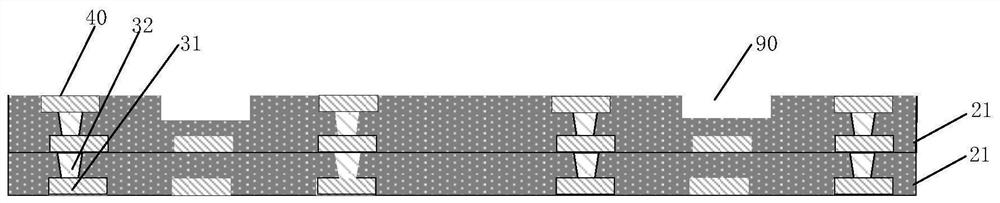
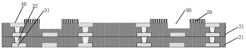
[0036] S01: Provide a PCB board, the surface of the PCB board has a plurality of grooves 90, and the surface of the PCB board is formed with a plurality of exposed first pads 40;

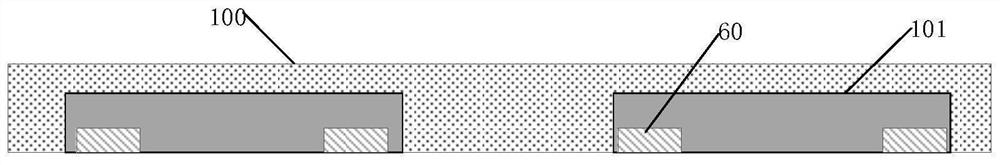
[0037] S02: Provide a device wafer 100, the device wafer 100 includes a plurality of first chips 101, and a plurality of exposed second pads 60 are formed on the surface of the first chips 101;

[0038] S03: bonding the device wafer 100 to the PCB board through the connection layer, the first pad 40 is opposite to the second pad 60 to form a gap 70a;

[0039] S04: The connection layer has a first opening at the position opposite to the groove 90, and the first opening and the groove 90 are jointly surrounded by the connection layer, the device wafer 100 and the PCB board to form a cavity 51, and the cavity 51 serves as the first chip 101 working chamber;

[0040] S05 : Fo...

Embodiment 2

[0077] refer to Image 6 , this embodiment 2 provides a system-in-package method, which is different from embodiment 1 in that: after forming the conductive bump 70, it also includes forming a via hole 80, the via hole 80 penetrates the device wafer 100 and extends to the first chip 101 superior.

[0078] In the present invention, a communication hole 80 is opened on the device wafer 100, which penetrates the device wafer 100 and extends to the first chip 101, so that the first chip 101 is exposed to the external atmosphere, thereby improving the working performance of the packaging structure and improving its utilization rate , and can be used in more occasions, making it more flexible.

[0079] Specifically, in this embodiment, at least one device wafer 100 is provided with a via hole 80 on the surface.

[0080] The other parts are the same as those in Embodiment 1, and will not be repeated here.

Embodiment 3

[0082] refer to Figure 5, Embodiment 3 provides a system-in-package structure, including:

[0083] A PCB board, the PCB board includes opposite front and back sides, the front side of the PCB board has a groove 90, and there are a plurality of exposed first welding pads 40 on the front side of the PCB board;

[0084] A device wafer 100, the device wafer 100 has a first chip 101, the surface of the device wafer 100 has a plurality of exposed second pads 60, the first pad 40 is arranged opposite to the second pad 60, the device wafer 100 Bonding on the surface of the PCB board through the connection layer, the first welding pad 40 is arranged opposite to the second welding pad 60;

[0085] The connection layer has a first opening at a position opposite to the groove 90, and the first opening and the groove 90 are jointly surrounded by the device wafer 100 and / or the PCB board to form a cavity 51, and the cavity 51 serves as a working cavity for the first chip 101;

[0086] Th...


PUM


Abstract

The invention provides a system-level packaging method and a packaging structure thereof. The method comprises the steps that a PCB is provided, the surface of the PCB is provided with a plurality of grooves, and a plurality of exposed first welding pads are formed on the surface of the PCB; a device wafer is provided, the device wafer comprises a plurality of first chips, and a plurality of exposed second welding pads are formed on the surfaces of the first chips; the connecting layer is provided with a first opening at a position opposite to the groove, and the first opening and the groove are jointly enclosed by the connecting layer, the device wafer and the PCB to form a cavity. The device wafer and the PCB are bonded through the connecting layer, the connecting layer is provided with the first opening, the PCB is provided with the groove, the groove and the first opening are oppositely arranged, when the device wafer and the PCB are bonded, the groove and the first opening are jointly enclosed by the connecting layer, the device wafer and the PCB to form the cavity, and the cavity provides a working cavity environment for the first chip. A sealing cover does not need to be additionally arranged, the process is simplified, the device integration height is reduced, the process difficulty is reduced, and the conductive performance of the packaging structure is improved.

Description

technical field [0001] The invention belongs to the technical field of semiconductors, and more specifically relates to a system-in-package method and a package structure thereof. Background technique [0002] System-in-Package adopts any combination to combine multiple active components / devices, passive components / devices, MEMS devices, discrete KGD (Known Good Die) such as optoelectronic chips, biochips, etc., with different functions and prepared by different processes. In three dimensions (X direction, Y direction and Z direction), it is integrated and assembled into a single standard package with a multi-layer device structure and can provide multiple functions to form a system or subsystem. [0003] Flip-chip (FC, Flip-Chip) soldering is a system-in-package method commonly used at present. The system-in-package method includes: providing a PCB circuit board, wherein solder balls arranged according to certain requirements are formed on the PCB circuit board (formed by ...

Claims


Application Information

Patent Timeline
Patent Type & Authority Applications(China)
IPC IPC(8): H01L21/50H01L21/60H01L23/488H01L25/16
CPCH01L21/50H01L24/81H01L23/488H01L25/16H01L2224/818
Inventor 蔺光磊
Owner 芯知微(上海)电子科技有限公司
Why Eureka
Try Eureka