System-level packaging method and packaging structure

A system-level packaging, plastic packaging layer technology, applied in the direction of assembling printed circuits with electrical components, printed circuits connected with non-printed electrical components, electrical components, etc., can solve the difficulty of process control, large package size, and packaging effect. It can improve the space utilization rate, reduce the bonding stress, and reduce the height.

Inactive Publication Date: 2021-10-26
芯知微(上海)电子科技有限公司
View PDF7 Cites 1 Cited by
  • Summary
  • Abstract
  • Description
  • Claims
  • Application Information

AI Technical Summary

Problems solved by technology

[0005] The purpose of the present invention is to provide a system-level packaging method and packaging structure, which can solve technical problems such as difficulty in process control, large packaging size, low integration, and poor packaging effect.

Method used


Image

  • System-level packaging method and packaging structure
  • System-level packaging method and packaging structure
  • System-level packaging method and packaging structure

Examples


Embodiment 1

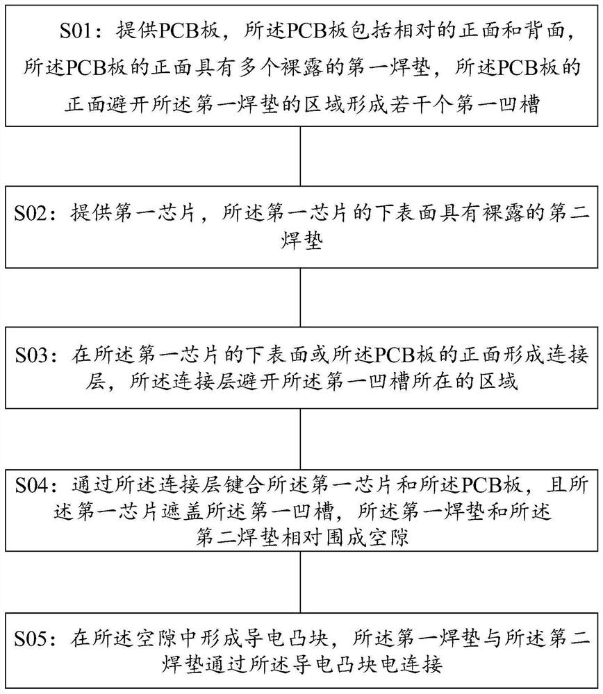
[0033] refer to figure 1 , this embodiment 1 provides a system-in-package method, including the following steps:

[0034] S01: Provide a PCB board, the PCB board includes opposite front and back sides, the front side of the PCB board has a plurality of exposed first pads, and the area of ​​the front side of the PCB board avoiding the first pads is formed with several first grooves;

[0035] S02: providing a first chip, the lower surface of the first chip has an exposed second pad;

[0036] S03: forming a connection layer on the lower surface of the first chip or the front surface of the PCB board, and the connection layer avoids the area where the first groove is located;

[0037] S04: bonding the first chip and the PCB board through the connection layer, and the first chip covers the first groove, and the first pad and the second pad relatively surround a gap;

[0038] S05: Form a conductive bump in the gap, and electrically connect the first pad and the second pad through ...

Embodiment 2

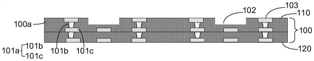
[0080] refer to Figure 7 and Figure 8 , this embodiment provides a system-in-package structure, Figure 7 A schematic diagram of a system-in-package structure of Embodiment 2 is shown, and the system-in-package structure includes:

[0081] PCB board 100, PCB board 100 comprises opposite front side 110 and back side 120, the front side 110 of PCB board 100 has a plurality of exposed first welding pads 103, the front side 110 of PCB board 100 avoids the area of ​​first welding pad 103 to form several a first groove 102;

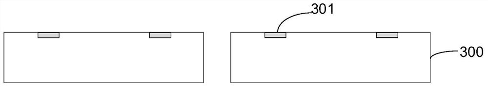
[0082] The first chip 300, the lower surface of the first chip 300 has an exposed second welding pad 301, the first chip 300 is bonded to the front side 110 of the PCB board 100 through the connection layer 200, the first welding pad 103 and the second welding pad 301 oppositely arranged, and the first chip 300 covers the first groove 102;

[0083] The conductive bump 400 b is disposed between the first pad 103 and the second pad 301 to electrically conne...

Embodiment 3

[0094] refer to Figure 9 This embodiment 3 provides a system-in-package structure. The difference from embodiment 2 is that the plastic encapsulation layer 500 is provided with a communication hole 501 , and the communication hole 501 penetrates the plastic encapsulation layer 500 and extends to the first chip 300 .

[0095] In this embodiment, the first chip 300 adopting the airtight cavity structure is a MEMS chip, and the MEMS chip that can also use the communication hole 501 to communicate with the outside world can be a sensor module chip, such as a temperature sensor, a heat flow sensor, a thermal conductivity sensor, At least one of a light modulator, an acoustic sensor, a gas sensor, a humidity sensor, an ion sensor, a biosensor, and the like. This embodiment is a microphone module chip, which receives sound waves through the communication hole 501 and transmits sound signals. The sensor module chips in the present invention are not limited to the types listed here, ...


PUM


Abstract

The invention provides a system-level packaging method and packaging structure, and the method comprises the steps: providing a PCB which comprises a front surface and a back surface which are opposite to each other, wherein the front surface of the PCB is provided with a plurality of exposed first welding pads and first grooves; providing a first chip, wherein the lower surface of the first chip is provided with an exposed second welding pad; forming a connecting layer on the lower surface of the first chip or the front surface of the PCB, wherein the connecting layer avoids the area where the first groove is located; bonding the first chip and the PCB through the connecting layer, wherein the first chip covers the first groove, and the first welding pad and the second welding pad oppositely define a gap; bonding the first welding pad and the second welding pad to the front surface of the PCB through the connecting layer and are opposite to define a gap; and forming a conductive bump in the gap through an electroplating process, wherein the first welding pad and the second welding pad are electrically connected through the conductive bump. The chips are bonded on the front surface and the back surface of the PCB, and the traditional step of bonding the chips on the wafer is omitted, so that the process is simplified, the process difficulty is reduced, and the integration level is improved.

Description

technical field [0001] The invention relates to the technical field of semiconductors, in particular to a system-in-package method and a package structure. Background technique [0002] System-in-Package adopts any combination to combine multiple active components / devices, passive components / devices, MEMS devices, discrete KGD (Known Good Die) such as optoelectronic chips, biochips, etc., with different functions and prepared by different processes. In three dimensions (X direction, Y direction and Z direction), it is integrated and assembled into a single standard package with a multi-layer device structure and can provide multiple functions to form a system or subsystem. [0003] Flip-chip (FC, Flip-Chip) soldering is a system-in-package method commonly used at present. The system-in-package method includes: providing a PCB circuit board, wherein solder balls arranged according to certain requirements are formed on the PCB circuit board (formed by using a ball planting pr...

Claims


Application Information

Patent Timeline
Patent Type & Authority Applications(China)
IPC IPC(8): H01L21/50H01L21/56H01L21/60H01L23/488H01L23/31H01L25/16H05K1/11H05K1/18H05K3/30
CPCH01L21/50H01L21/56H01L24/81H01L23/488H01L23/3114H01L25/16H05K3/301H05K1/111H05K1/181H01L2224/818
Inventor 蔺光磊
Owner 芯知微(上海)电子科技有限公司
Why Eureka
Try Eureka