Wafer-level system packaging structure and method

A system packaging, wafer-level technology, applied in microstructure technology, microstructure devices, manufacturing microstructure devices, etc., can solve the problems of low packaging efficiency, large packaging size, and difficult process, so as to improve packaging efficiency and reduce High, simplified process effect

Inactive Publication Date: 2022-07-29
NINGBO SEMICON INT CORP
View PDF0 Cites 0 Cited by
  • Summary
  • Abstract
  • Description
  • Claims
  • Application Information

AI Technical Summary

Problems solved by technology

[0005] The purpose of the present invention is to provide a wafer-level system packaging structure and method, which at least solve the technical problems of low integration, large packaging size, difficult manufacturing process and low packaging efficiency

Method used


Image

  • Wafer-level system packaging structure and method
  • Wafer-level system packaging structure and method
  • Wafer-level system packaging structure and method

Examples


Embodiment 1

[0031] This embodiment 1 provides a wafer-level packaging method, which includes the following steps:

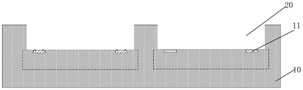
[0032] S01: Provide a device wafer, the surface of the device wafer has a plurality of exposed first pads, the surface of the device wafer forms a first cavity, and at least part of the first pads are located in the first below the cavity;

[0033] S02: providing a first chip, the surface of the first chip has a plurality of exposed second pads;

[0034] S03: Bond the first chip to the bottom of the first cavity through a connection layer, the connection layer has a first opening, and the first opening is covered by the first chip and / or the device wafer forming a second cavity, the second cavity is used as a working cavity of the first chip, and the first pad is opposite to the second pad to form a gap;

[0035] S04: A first conductive bump is formed in the gap by an electroplating process, and the first bonding pad and the second bonding pad are electrically connected th...

Embodiment 2

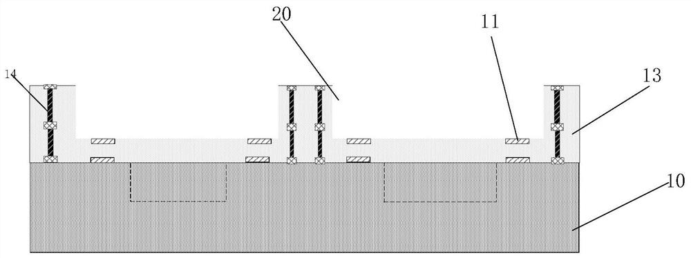
[0086] refer to Figure 11 , the difference from the first embodiment is that the backside of the device wafer 10 further includes a third pad 12 , and the third pad 12 is located on the interconnect structure in the device wafer 10 and on the surface of the second chip 80 . The formed fourth pads 81 are electrically connected, the third pads 12 and the fourth pads 81 are arranged opposite to each other, and are formed between the third pads 12 and the fourth pads 81 during the electroplating process The second conductive bumps 90 . In other embodiments, before or after the first conductive bumps 11 are formed, the third pads 12 and the fourth pads 81 may be connected by conductive materials such as solder balls and conductive pillars.

[0087] The exposed area of ​​the third pad 12 or the fourth pad 81 is 5-200 square microns. Within this range, the pad can be in sufficient contact with the electroplating solution to avoid the influence of insufficient contact between the pa...

Embodiment 3

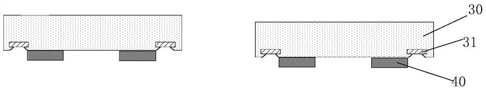
[0089] refer to Figure 12 , and the difference from the first embodiment is that a third chip 60 is bonded on the first chip 30 , and the third chip 60 is electrically connected to the first chip 30 . Specifically, the second surface of the first chip 30 includes a fifth bonding pad 32 , and the fifth bonding pad 32 is electrically connected to the first chip 30 , and the electrical connection may be realized by interconnecting wires inside the first chip 30 . The electrical connection can also be achieved by plugs, which is not limited here. The sixth pad 61 is formed on the surface of the third chip 60, and the fifth pad 32 and the sixth pad 61 are oppositely arranged. According to the electroplating process, a third conductive bump 70 is formed between the fifth bonding pad 32 and the sixth bonding pad 61; the third chip 60 and the first chip 30 can also be electrically connected through an electroless plating process, such as refer to Figure 13 , the third chip 60 and ...


PUM

PropertyMeasurementUnit
thicknessaaaaaaaaaa
areaaaaaaaaaaa
thicknessaaaaaaaaaa

Abstract

The invention relates to a wafer-level system packaging structure and method, and the method comprises the steps: providing a device wafer, the surface of the device wafer is provided with a plurality of exposed first welding pads, the surface of the device wafer is provided with a first cavity, and at least part of the first welding pads are located below the first cavity; providing a first chip, wherein the surface of the first chip is provided with a plurality of exposed second welding pads; the first chip is bonded to the bottom of the first cavity through a connecting layer with a first opening, a second cavity is defined by the first opening, the second cavity serves as a working cavity of the first chip, and a first conductive protruding block is formed through the electroplating technology so as to be electrically connected with the first welding pad and the second welding pad. According to the invention, the first cavity is formed on the device wafer, and the first chip is bonded at the bottom of the first cavity, so that the connection between the first chip and the device wafer is realized, the integration height of the device is reduced, and the space utilization rate is improved; and secondly, the second cavity is formed in the connecting layer, the second cavity provides a working cavity environment for the first chip, a sealing cover does not need to be additionally arranged, and the process is simplified.

Description

technical field [0001] The invention relates to the field of semiconductor manufacturing, in particular to a wafer-level system packaging structure and method. Background technique [0002] With the advent of the era of 5G communication and artificial intelligence (AI), the amount of data to be transmitted and processed by high-speed interactive processing of chips used in such related fields is very large, and the demand for mobile Internet and Internet of Things is getting stronger and stronger. Electronic terminal products The miniaturization and multi-functionalization of products have become the general trend of industrial development. How to integrate and package different types of high-density chips together to form a system or subsystem with powerful functions and relatively low volume power consumption has become a major challenge in the field of advanced semiconductor chip packaging. [0003] At present, the multi-chip integrated packaging for such high-density ch...

Claims


Application Information

Patent Timeline
Patent Type & Authority Applications(China)
IPC IPC(8): H01L21/60H01L21/52H01L23/488B81B7/00B81B7/02B81C1/00B81C3/00
CPCH01L24/81H01L24/82H01L24/11H01L24/83H01L21/52H01L24/32H01L24/16B81C1/00095B81C1/00047B81C1/00261B81B7/0006B81B7/02B81C3/001H01L2224/11462H01L2224/16145H01L2224/32148
Inventor 黄河向阳辉刘孟彬
Owner NINGBO SEMICON INT CORP
Why Eureka
Try Eureka