Small semiconductor device with wireless communication function

A wireless communication and semiconductor technology, applied in the direction of semiconductor devices, semiconductor/solid-state device components, electric solid-state devices, etc., can solve the problems of unusable semiconductor devices, waste of semiconductor devices, etc., to prevent perforation and wear, prevent water Damage, improve the effect of fault tolerance

Inactive Publication Date: 2021-10-22
WUXI TAIHU UNIV
View PDF0 Cites 0 Cited by
  • Summary
  • Abstract
  • Description
  • Claims
  • Application Information

AI Technical Summary

Problems solved by technology

However, the pin length of existing semiconductor devices is fixed. When the pins are broken or the pins are misplaced, the semiconductor devices cannot be used due to the fixed length of the pins, which in turn causes waste of semiconductor devices.

Method used


Image

  • Small semiconductor device with wireless communication function
  • Small semiconductor device with wireless communication function
  • Small semiconductor device with wireless communication function

Examples


Embodiment 1

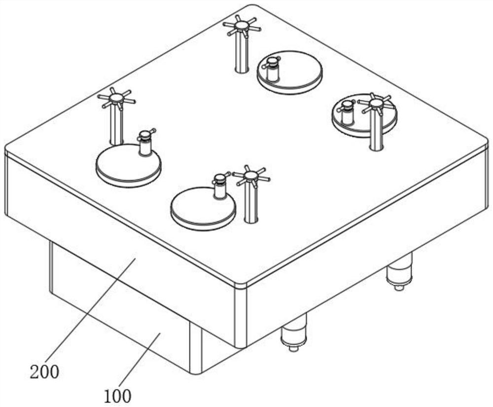
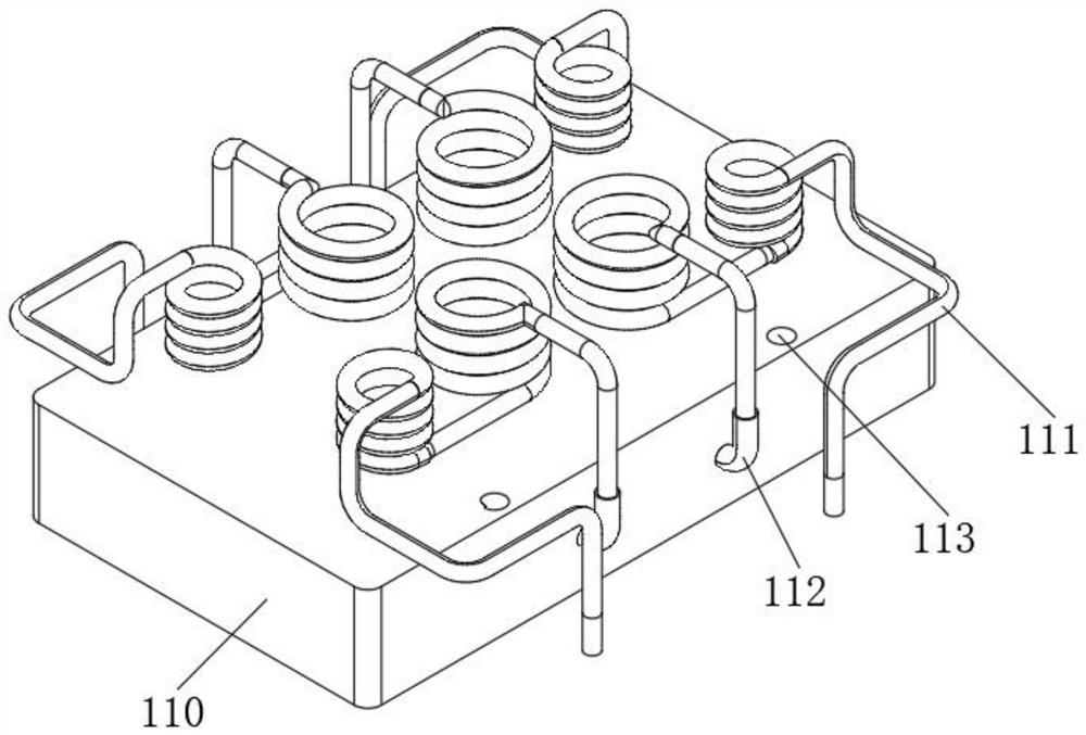
[0044] see Figure 1-Figure 7 As shown, a small semiconductor device with wireless communication function is provided, including a semiconductor device body 100 and an adjustment device 200 arranged above the semiconductor device body 100, the semiconductor device body 100 includes a housing 110, and the side wall of the housing 110 is connected with leads Foot 111, adjustment device 200 includes at least:

[0045] The storage mechanism 210, the storage mechanism 210 includes a fixed shell 211, the fixed shell 211 is fixed on the top of the housing 110, the bottom of the fixed shell 211 is provided with a plurality of perforations 212, the perforations 212 are slidably connected to one end of the pin 111, and the bottom of the fixed shell 211 The inner wall is provided with a plurality of square plates 213, and the square plates 213 are in an annular structure. A storage cavity is formed between the inside of the square plate 213 and the bottom of the fixed shell 211. The pins...

Embodiment 2

[0053] In order to realize the protection of pin 111, the following improvements are made on the basis of Embodiment 1:

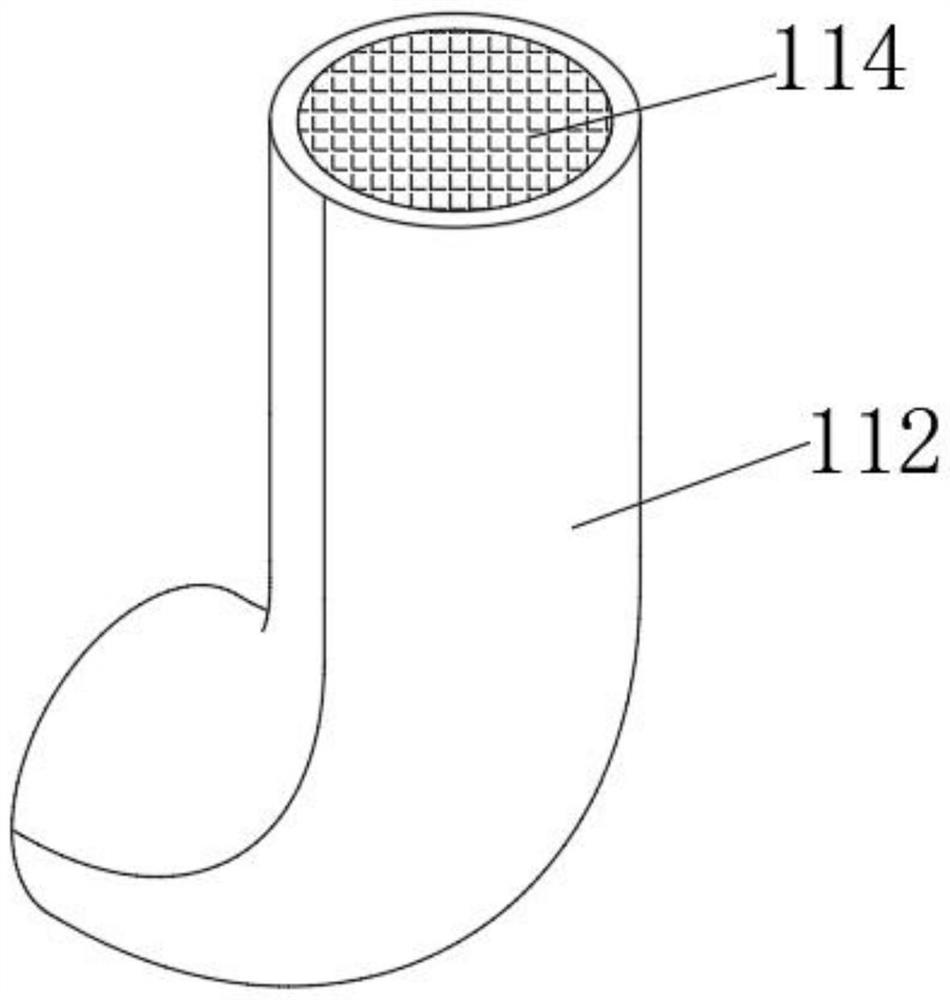
[0054] see Figure 8 As shown, wherein, the bottom of the fixed shell 211 is fixedly connected to the outer ring of the perforation 212 with a sleeve 230, and a sliding cavity is opened between the inner wall and the outer wall of the sleeve 230, and a protective ring 231 is slidably connected in the sliding cavity. When the pin 111 is installed, the protective ring 231 slides out to cover one end of the pin 111, so that the external water source cannot be in contact with the pin 111, thereby preventing the pin 111 from being damaged by water and realizing the protection of the pin 111. protection of.

[0055] Further, in order to improve the protective performance of the protective ring 231 on the pin 111, one end of the sleeve 230 is fixedly connected to a return spring 232 in the sliding cavity, and one end of the return spring 232 is fixedly connected ...

Embodiment 3

[0057] In order to adjust the height of the adjusting device 200, the following improvements are made on the basis of Embodiment 1:

[0058] see Figure 9 As shown, wherein, the surface of the casing 110 is provided with a rotary hole 113, and a threaded rod 240 is rotatably connected in the rotary hole 113. The threaded rod 240 passes through the bottom of the fixed shell 211, and the threaded rod 240 is screwed to the bottom of the fixed shell 211. When When the height needs to be adjusted, screw the threaded rod 240, and the rotation of the threaded rod 240 drives the fixed shell 211 to move up, thereby realizing the height adjustment of the adjusting device 200, so that the height of the adjusting device 200 can be adjusted when the installation space is small. To reduce the space occupied by the semiconductor device body 100 and realize installation in different environments.

[0059] In addition, in order to rotate the threaded rod 240 easily and quickly, a slot is prov...


PUM


Abstract

The invention relates to the technical field of semiconductor devices, in particular to a small semiconductor device with a wireless communication function. The small semiconductor device with a wireless communication function comprises a semiconductor device body and an adjusting device arranged above the semiconductor device body, the semiconductor device body comprises a shell, the side wall of the shell is connected with pins, the adjusting device at least comprises a storage mechanism, the storage mechanism comprises a fixed shell, and the fixed shell is fixed to the top of the shell. According to the small semiconductor device with the wireless communication function, the pin with the redundant length is stored through the arranged adjusting device, and the stored pin can be pulled out when the pin is broken, so that the error-tolerant rate of mounting the semiconductor device is improved, and the problems that the length of the pin of the existing semiconductor device is fixed, and when the pin is broken or the pins are installed in a staggered manner, due to the fact tjat the length of the pins is fixed, the semiconductor device cannot be continuously used can be solved, and the problem of waste of the semiconductor device is further caused.

Description

technical field [0001] The invention relates to the technical field of semiconductor devices, in particular to a small semiconductor device with a wireless communication function. Background technique [0002] A semiconductor device is an electronic device whose conductivity is between a good conductor and an insulator. It uses the special electrical properties of semiconductor materials to complete specific functions. It can be used to generate, control, receive, transform, amplify signals and perform energy conversion. [0003] In recent years, with the rapid development of the semiconductor industry, the functions of its semiconductor devices have also increased, such as adding wireless communication functions to semiconductor devices to increase the identification of its information. However, the pin length of the existing semiconductor device is fixed. When the pin is broken or the pin is misplaced, the semiconductor device cannot be used continuously due to the fixed l...

Claims


Application Information

Patent Timeline
Patent Type & Authority Applications(China)
IPC IPC(8): H01L23/49H01L23/10
CPCH01L23/49H01L23/10
Inventor 尹嵘顾吉朱妍陈熹程岩
Owner WUXI TAIHU UNIV
Why Eureka
Try Eureka