Laminating method of copper-clad plate and circuit board
A technology for copper clad laminates and circuit boards, which is used in multilayer circuit manufacturing, circuit lamination, printed circuits, etc., can solve the problems affecting the uniformity of dielectric thickness and the bending deformation of the core board, so as to ensure the uniformity and alleviate the bending deformation. effect of stress
- Summary
- Abstract
- Description
- Claims
- Application Information
AI Technical Summary
Problems solved by technology
Method used
Image

Examples
Embodiment Construction
[0020] In order to make the technical problems solved by the present application, the technical solutions adopted and the technical effects achieved clearer, the technical solutions of the embodiments of the present application will be further described in detail below in conjunction with the accompanying drawings.
[0021] Reference herein to an "embodiment" means that a particular feature, structure, or characteristic described in connection with the embodiment can be included in at least one embodiment of the present application. The occurrences of this phrase in various places in the specification are not necessarily all referring to the same embodiment, nor are separate or alternative embodiments mutually exclusive of other embodiments. It is understood explicitly and implicitly by those skilled in the art that the embodiments described herein can be combined with other embodiments.
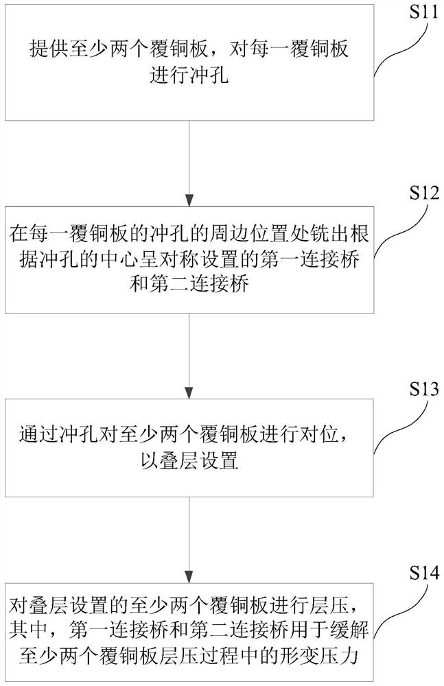
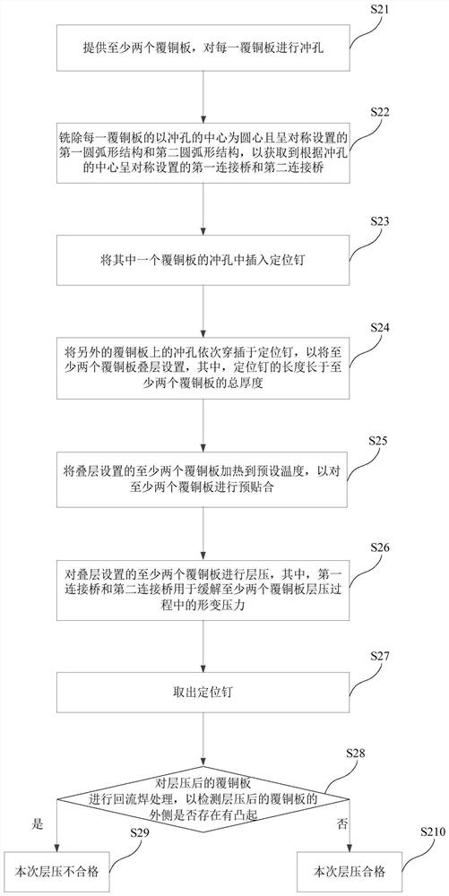
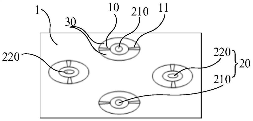
[0022] see figure 1 , figure 1 It is a schematic flow chart of the first embodiment of...
PUM
 Abstract
Description
Claims
Application Information
 - R&D Engineer
- R&D Manager
- IP Professional
- Industry Leading Data Capabilities
- Powerful AI technology
- Patent DNA Extraction
Browse by: Latest US Patents, China's latest patents, Technical Efficacy Thesaurus, Application Domain, Technology Topic.
© 2024 PatSnap. All rights reserved.Legal|Privacy policy|Modern Slavery Act Transparency Statement|Sitemap