Light-emitting device and display panel

A technology of light-emitting devices and substrates, applied in optical components, electric solid-state devices, semiconductor devices, etc., can solve problems such as waste, and achieve the effect of improving the coupling light efficiency

Active Publication Date: 2021-10-26
BOE TECH GRP CO LTD
View PDF9 Cites 0 Cited by
  • Summary
  • Abstract
  • Description
  • Claims
  • Application Information

AI Technical Summary

Problems solved by technology

[0005] In order to solve the technical problem that the light emitted by the existing light emitting device is wasted in the plasmon mode, the main purpose of this application is to provide a light emitting device and a display panel

Method used


Image

  • Light-emitting device and display panel
  • Light-emitting device and display panel
  • Light-emitting device and display panel

Examples


Embodiment 1

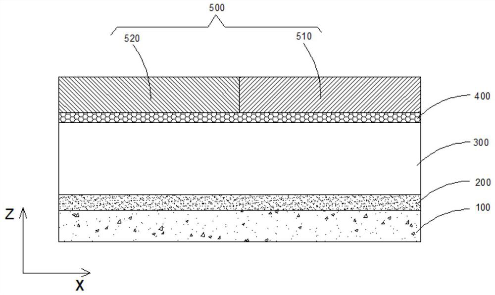
[0035] combine figure 1 and Figure 7 As shown, the embodiment of the present application provides a light-emitting device and a display panel. The display panel is equipped with the light-emitting device. The light-emitting device includes a substrate 100. The substrate 100 is formed with a pixel area that emits light of one color. The group of the first electrode layer 200, the organic functional layer 300, the second electrode layer 400, and the light-exiting layer 500, the group of the light-exiting layer 500 includes the first coupling layer 510 and the second coupling layer 520 whose refractive index is smaller than the first coupling layer 510, the second A coupling layer 510 and the second coupling layer 520 are located on the same layer and adjacent to each other, thereby dividing the pixel area into two light output areas, the first coupling layer 510 is located in one of the light output areas, and the second coupling layer 520 is located in the other light output a...

Embodiment 2

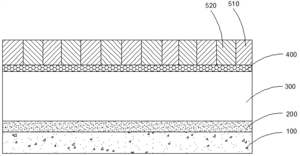
[0040] combine figure 2 and Figure 7 As shown, the embodiment of the present application provides a light-emitting device and a display panel. The display panel is equipped with the light-emitting device. The light-emitting device includes a substrate 100. The substrate 100 is formed with a pixel area that emits light of one color. The group of the first electrode layer 200, the organic functional layer 300, the second electrode layer 400 and the light output layer 500, the group of the light output layer 500 includes a plurality of first coupling layers 510 and second coupling layers 520 arranged alternately in the same layer, and the second The coupling layer 520 has a lower refractive index than the first coupling layer 510 .

[0041] In the embodiment of the present application, multiple pixel areas can be formed, and each pixel area only emits light of one color, and the top layer interface of the second electrode layer 400 interacts with photons, thereby forming Surf...

Embodiment 3

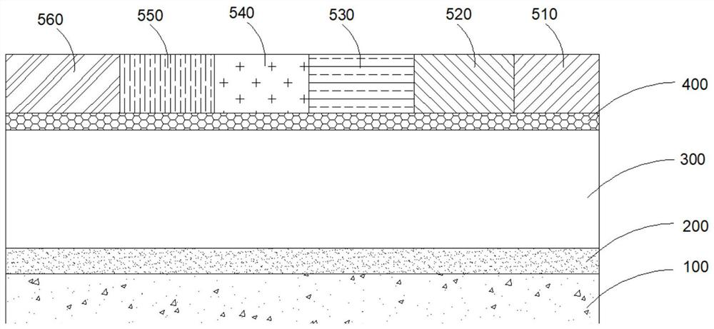
[0043] combine image 3 and Figure 7 As shown, the embodiment of the present application provides a light-emitting device and a display panel. The display panel is equipped with the light-emitting device. The light-emitting device includes a substrate 100. The substrate 100 is formed with a pixel area that emits light of one color. The first electrode layer 200, the organic functional layer 300, the second electrode layer 400, and the light-exiting layer 500 group, the light-exiting layer 500 group includes a plurality of coupling layers arranged in the same layer, and the refractive index between each coupling layer is different, so that the phase One of the adjacent coupling layers has a high refractive index and the other has a low refractive index.

[0044] Surface plasmons are formed in the coupling layer with a low refractive index. The dispersion curve of the surface plasmons does not intersect with the dispersion curve of the coupling layer in the region, and the sur...


PUM


Abstract

The invention generally relates to the technical field of display, in particular to a light-emitting device and a display panel, the display panel is provided with the light-emitting device, the light-emitting device comprises a substrate, a pixel area emitting light of one color is formed on the substrate, the pixel region comprises a first electrode layer, an organic functional layer, a second electrode layer and a light emitting layer group which are far away from the substrate, the light emitting layer group comprises at least two coupling layers with different refractive indexes, and the refractive indexes of the two adjacent coupling layers are different; and after light in a surface plasmon polariton mode is transmitted from the coupling layer with the low refractive index to the coupling layer with the high refractive index, a dispersion curve of surface plasmon polaritons and a dispersion curve of the coupling layer with the high refractive index have an intersection point, wave vector matching is achieved, light is radiated in the coupling layer with the high refractive index, and therefore the coupling light emitting efficiency is improved.

Description

technical field [0001] The present application generally relates to the field of display technology, and in particular, relates to a light emitting device and a display panel. Background technique [0002] Due to the advantages of light weight, fast response, low operating voltage, wide color gamut, wide viewing angle, high brightness, and low power consumption, organic light-emitting diodes (OLEDs) have attracted extensive attention from researchers in lighting and flat panel display applications in recent years. . [0003] However, a serious problem in OLED devices is that most of the light generated in the active layer of the device is wasted in the surface plasmon mode. Organic light-emitting diodes with high coupling-out efficiency have always been the focus of research in this field. Contents of the invention [0004] A series of concepts in simplified form are introduced in the Summary of the Invention, which will be further detailed in the Detailed Description. T...

Claims


Application Information

Patent Timeline
Patent Type & Authority Applications(China)
IPC IPC(8): H01L51/52G02B5/00
CPCG02B5/008H10K50/858
Inventor 樊燕温向敏
Owner BOE TECH GRP CO LTD
Why Eureka
Try Eureka