Transmitter with low-speed SerDes interface, receiver and circuit design method thereof
A transmitter and receiver technology, applied in the field of SerDes, can solve problems such as high cost and high risk of adapting new technologies, and achieve the effects of ensuring integrity, reducing design risk and cost, and ensuring no error codes
- Summary
- Abstract
- Description
- Claims
- Application Information
AI Technical Summary
Problems solved by technology
Method used
Image

Examples
Embodiment 1
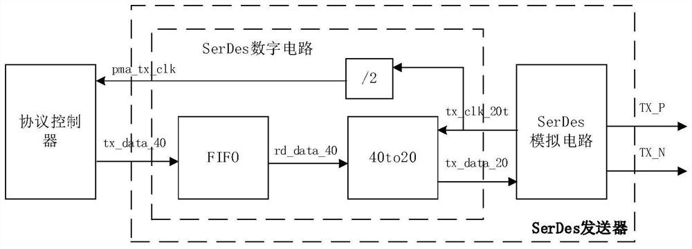
[0043] The basic structure of the existing SerDes transmitter circuit is as follows: figure 1 As shown, the SerDes analog part circuit generates the SerDes parallel data transmission clock tx_clk_20t according to the rate configuration. The clock frequency is the rate / parallel data bit width, and the SerDes parallel data bit width is 20 bits. Therefore, when the rate configuration is 8.5G, tx_clk_20t = 425Mhz (8.5 G / 20bit); when the rate configuration is 4.25G, tx_clk_20t = 212.5Mhz (4.25G / 20bit); when the rate configuration is 2.125G, tx_clk_20t = 106.25Mhz (2.125G / 20bit). Since the FC controller transmits data with a parallel bit width of 40 bits, the SerDes digital part first divides tx_clk_20t by two to generate the controller’s parallel data transmission clock pma_tx_clk (53.125Mhz) and inputs it to the FC controller for 40-bit parallel data transmission, and then the FC The data sent by the controller is read across asynchronously through the asynchronous FIFO, and then ...
Embodiment 2
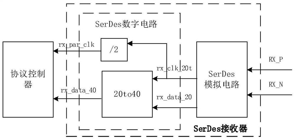
[0046] The basic structure of the existing SerDes receiver circuit is as follows: image 3 As shown, the SerDes analog part circuit generates the SerDes parallel data receiving clock rx_clk_20t according to the rate configuration. The clock frequency is rate / parallel data bit width, and the SerDes parallel data bit width is 20 bits. Therefore, when the rate configuration is 8.5G, rx_clk_20t = 425Mhz (8.5 G / 20bit); when the rate configuration is 4.25G, rx_clk_20t = 212.5Mhz (4.25G / 20bit); when the rate configuration is 2.125G, rx_clk_20t = 106.25Mhz (2.125G / 20bit). The SerDes analog circuit first converts the high-speed differential serial data received from RX_P / RX_N into 20-bit parallel data rx_data_20, and at the same time generates a 20t SerDes parallel data receiving clock rx_clk_20t. Since the FC controller receives data parallel bit width is 40 bits, the SerDes digital First, rx_clk_20t is divided by two to generate the parallel data receiving clock rx_par_clk (53.125Mhz...
Embodiment 3
[0049] Based on the same design principle as Embodiment 1, this embodiment of the present invention also provides a transmitter with a 1.25Gbps low-speed SerDes interface. The difference from Embodiment 1 is that this embodiment of the present invention is based on the existing 2.5Gbps SerDes transmitter circuit For the design, the rate of the SerDes analog circuit is configured to be 2.5Gbps, and the protocol controller is adjusted to be an SRIO controller. The other contents are the same as those in Embodiment 1, and will not be repeated here.
PUM
 Abstract
Description
Claims
Application Information