Substrate and display panel

A substrate and semiconductor technology, used in instruments, electrical components, electrical solid-state devices, etc., can solve the problem of large size of electrostatic protection devices

CN113594139APending Publication Date: 2021-11-02SHENZHEN CHINA STAR OPTOELECTRONICS SEMICON DISPLAY TECH CO LTD
8 Cites 0 Cited by

Patent Information

Authority / Receiving Office
CN · China
Patent Type
Applications(China)
Current Assignee / Owner
Publication Date
2021-11-02

Smart Images

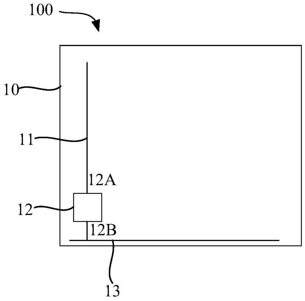
  • Figure 1
    Figure 1
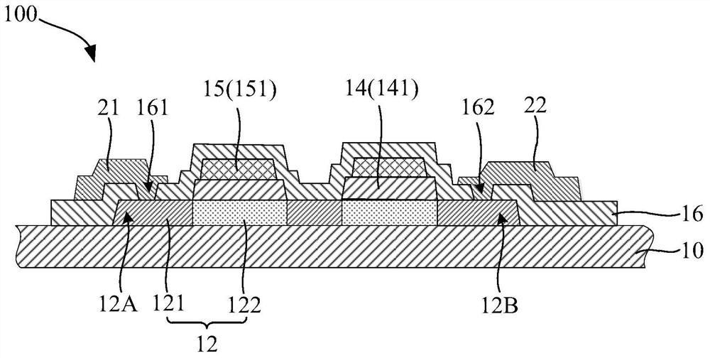
  • Figure 2
    Figure 2
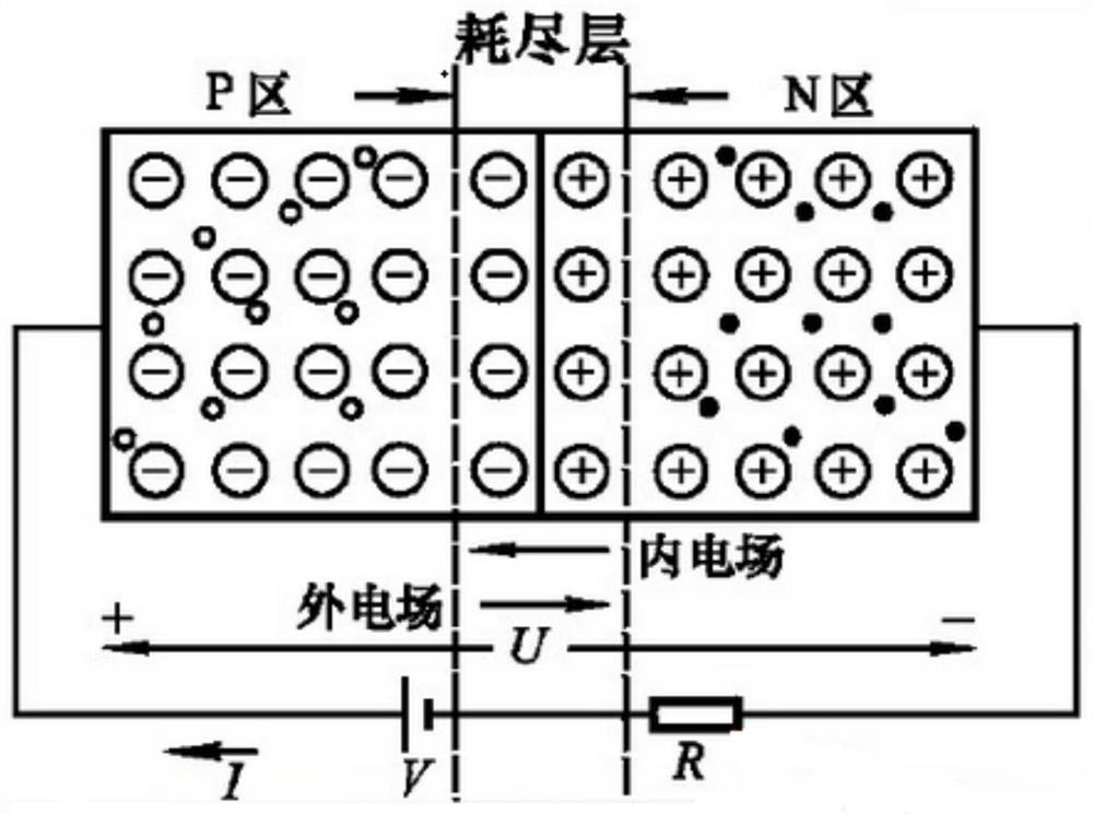
  • Figure 3
    Figure 3
Patent Text Reader

Abstract

The invention discloses a substrate and a display panel. The substrate comprises a substrate, a signal line, an electrostatic protection device and a common electrode line. The electrostatic protection device comprises a plurality of first semiconductors and second semiconductors, the first semiconductors and the second semiconductors are alternately arranged, the adjacent first semiconductors and the second semiconductors are in contact connection, and the types of the first semiconductors and the types of the second semiconductors are different. In the alternate arrangement and extension direction of the first semiconductors and the second semiconductors, the electrostatic protection device is provided with a head end and a tail end, the signal line is connected with the head end, and the common electrode line is connected with the tail end. The electrostatic protection device provided by the invention is very small in size, and is favorable for realizing a narrow frame of the display panel.
Need to check novelty before this filing date? Find Prior Art

Description

technical field

[0001] The present application relates to the field of display technology, in particular to a substrate and a display panel. Background technique

[0002] Electro Static Discharge (ESD) is a common phenomenon, and the electrostatic problem directly affects the production yield of the display device. Usually, a static protection circuit is arranged around the display substrate to release or equalize high-voltage static electricity, so that the display device is protected from static electricity damage during production, transportation and operation.

[0003] Among them, the electrostatic protection circuit usually uses a thin film transistor as the main device for electrostatic protection. Currently, existing discharge device designs include diode-connected transistors (Diode TFTs) and floating transistors (Floating TFTs). However, in order to meet the requirement of electrostatic protection, the size of the thin film transistor will be designed relatively l...

Examples

Embodiment Construction

[0042] The following will clearly and completely describe the technical solutions in the embodiments of the application with reference to the drawings in the embodiments of the application. Apparently, the described embodiments are only some of the embodiments of the application, not all of them. Based on the embodiments in this application, all other embodiments obtained by those skilled in the art without making creative efforts belong to the scope of protection of this application. In addition, it should be understood that the specific implementations described here are only used to illustrate and explain the present application, and are not intended to limit the present application. In this application, unless stated otherwise, the used orientation words such as "up", "down", "left", and "right" usually refer to the upper, lower, and left sides in the actual use or working state of the device. and right, specifically the direction of the drawing in the attached drawing.

...