Display substrate, display panel and display device

A technology for displaying substrates and substrates, applied to static indicators, static electricity, electrical components, etc., to achieve the effects of improving vertical lines, preventing burnout, and enhancing antistatic capabilities

Pending Publication Date: 2021-11-09
BOE TECH GRP CO LTD +1
View PDF0 Cites 0 Cited by
  • Summary
  • Abstract
  • Description
  • Claims
  • Application Information

AI Technical Summary

Problems solved by technology

[0003] Embodiments of the present disclosure provide a display substrate, a display panel and a display device to solve or alleviate one or more technical problems in the prior art

Method used


Image

  • Display substrate, display panel and display device
  • Display substrate, display panel and display device
  • Display substrate, display panel and display device

Examples


Embodiment Construction

[0034] In the following, only some exemplary embodiments are briefly described. As those skilled in the art would realize, the described embodiments may be modified in various different ways, all without departing from the spirit or scope of the present disclosure. Accordingly, the drawings and descriptions are to be regarded as illustrative in nature and not restrictive.

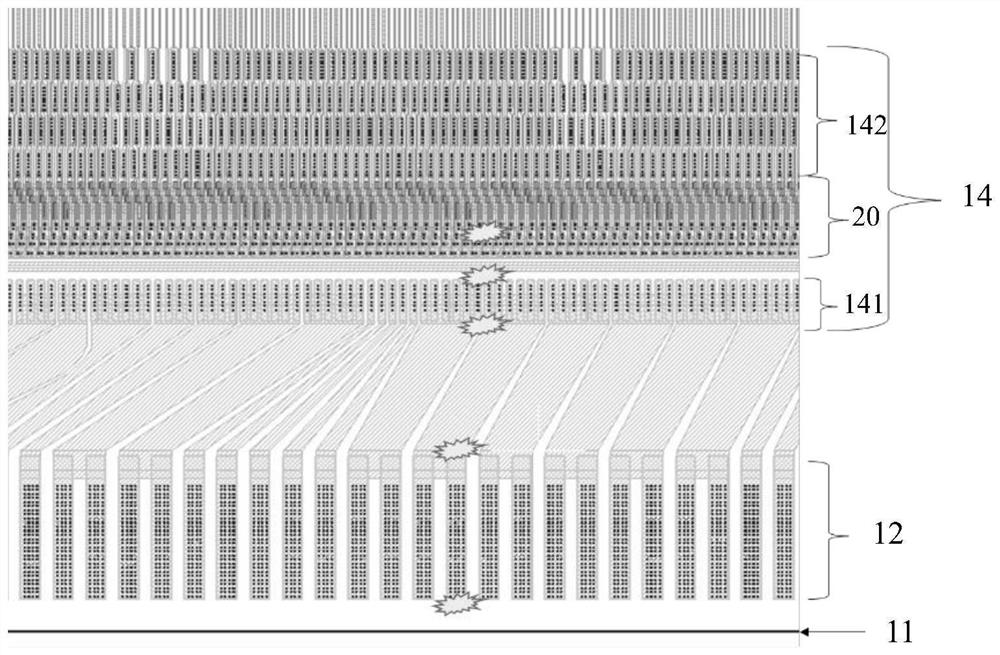
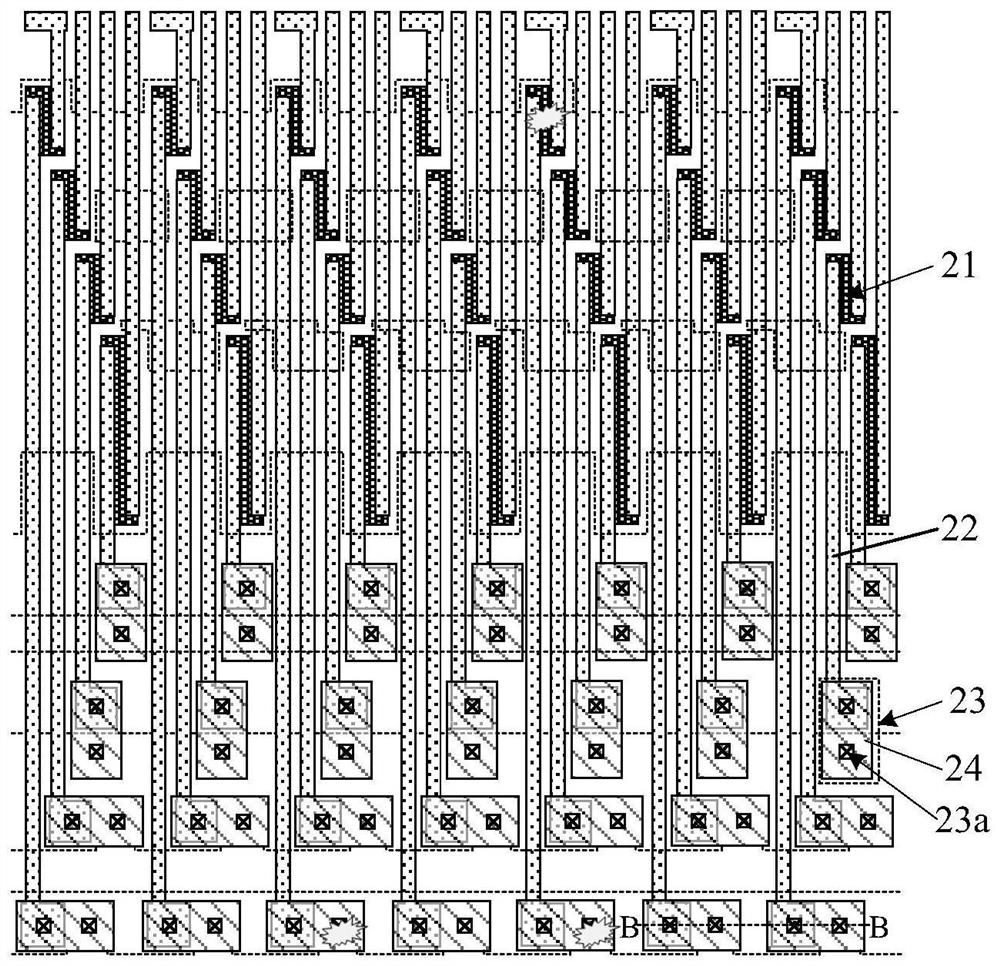
[0035] figure 1 is a schematic diagram showing the frame area of ​​the substrate, figure 2 for figure 1 The enlarged schematic diagram of the detection circuit area in the related art. Such as figure 1 As shown, the display substrate has a first edge 11, and the frame area may include a flexible circuit board pin area 12 and a driver chip setting area 14 arranged in sequence from the first edge 11 toward the inner side of the display substrate. The driver chip setting area 14 may include a driver chip input pin area 141 , a detection circuit area 20 and a driver chip output pin area 142 arranged in se...


PUM


Abstract

The embodiment of the invention provides a display substrate, a display panel and a display device. The display substrate is provided with a detection circuit used for detecting the display substrate, the detection circuit comprises a plurality of switching devices, a plurality of detection signal patch cords and a plurality of patch hole pairs, and the switching devices, the detection signal patch cords and the patch hole pairs are in one-to-one correspondence, each switching device is connected with the corresponding switching hole pair through the corresponding detection signal switching line, and at least two switching hole pairs in the switching hole pairs used for being connected with the same detection input signal are connected into an integrated structure through conductive connecting lines. According to the technical scheme, static electricity can be dispersed, the antistatic capacity of the product is enhanced, the burning phenomenon is prevented, the poor vertical line of the product is improved, and the reactivation rate of the product is increased.

Description

technical field [0001] The present disclosure relates to the field of display technology, and in particular to a display substrate, a display panel and a display device. Background technique [0002] Before the display device becomes a finished product, the display substrate needs to be inspected. Therefore, a detection circuit is provided at a corresponding position of the display substrate, and the detection circuit includes a detection circuit device. The detection circuit device (such as a thin film transistor) is connected to the transfer hole through a detection signal transfer line, and the transfer hole is used to connect to an externally input detection signal. However, static electricity will be generated during the manufacturing process of the display substrate, and the static electricity will be transmitted from the outside to the transfer hole through the flexible circuit board pin (FPC bump) and the driver chip input pin (IC input bump) on the display substrate...

Claims


Application Information

Patent Timeline
Patent Type & Authority Applications(China)
IPC IPC(8): G09G3/20H05F3/00
CPCG09G3/20H05F3/00G09G2330/12
Inventor 董职福王孝林王武
Owner BOE TECH GRP CO LTD
Why Eureka
Try Eureka