Ambient light compensation circuit for infrared receiving device

A technology of infrared receiving and compensating circuits, which is applied in the direction of adjusting electrical variables, without intermediate conversion to AC conversion equipment, instruments, etc., and can solve the problem that the receiving device cannot apply a linear amplification system.

Active Publication Date: 2021-11-09
WUXI CRYSTAL SOURCE MICROELECTRONICS CO LTD
View PDF4 Cites 1 Cited by
  • Summary
  • Abstract
  • Description
  • Claims
  • Application Information

AI Technical Summary

Problems solved by technology

[0005] Through the above process, it can be seen that for different ambient light current IF, the gain of the device changes, tha

Method used


Image

  • Ambient light compensation circuit for infrared receiving device
  • Ambient light compensation circuit for infrared receiving device
  • Ambient light compensation circuit for infrared receiving device

Examples


Embodiment Construction

[0039] The present invention will be described in detail below in conjunction with the implementations shown in the accompanying drawings, but it should be noted that these implementations are not limitations of the present invention, and those of ordinary skill in the art based on the functions, methods, or structural changes made by these implementations Equivalent transformations or substitutions all fall within the protection scope of the present invention.

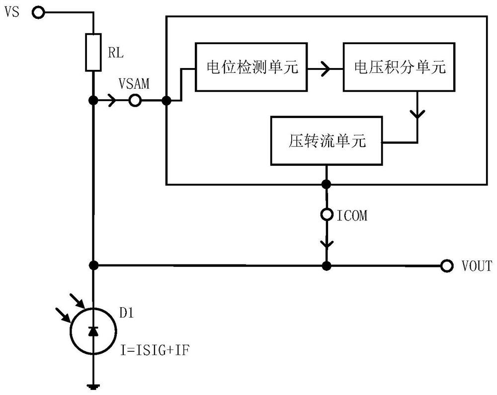
[0040] Such as figure 2 , image 3 As shown, the ambient light compensation circuit for the infrared receiving device of the present invention includes an infrared receiving diode D1 and a load resistor RL, including:

[0041]A potential detection unit, the signal input terminal of the potential detection unit is connected to the first voltage signal output terminal VSAM, and the first voltage signal output terminal VSAM is connected to the common end of the infrared receiving diode D1 and the load resistor RL, and ...


PUM


Abstract

The invention relates to an ambient light compensation circuit for an infrared receiving device. The circuit comprises a potential detection unit, a voltage integration unit and a voltage-current conversion unit which are connected in sequence, wherein the potential detection unit is used for receiving a first voltage signal (VSAM) and comparing the first voltage signal (VSAM) with a reference voltage; the voltage integration unit comprises a first switch (SW1) for controlling the charging of a capacitor and a second switch (SW2) for controlling the discharging of the capacitor, and the first switch (SW1) and the second switch (SW2) are controlled according to an output signal of the potential detection unit, so that the capacitor is charged or discharged to output a second voltage signal (VX); and the voltage-current conversion unit is used for converting the second voltage signal (VX) to output a compensation current. According to the invention, the ambient light current compensation can be realized, and the stable gain is realized.

Description

technical field [0001] The invention relates to an ambient light compensation circuit for an infrared receiving device. Background technique [0002] Such as figure 1 As shown, the circuit structure of the traditional infrared receiving device includes: photosensitive tube D1, load resistors R1, R2...RN, bypass tubes N1, N2...NN, voltage source VDD, internal reference source VS, and output terminal VOUT. [0003] The working process of this structure is: the photosensitive tube D1 receives the infrared signal, and generates the infrared receiving current I=ISIG+IF (ISIG is the signal current, IF is the ambient light current, ISIG<<IF), and the current is in the resistance R1, R2...RN A signal voltage is formed on it. [0004] When the current I is small, VOUT=VS-I*(R1+R2+…+RN), its gain is 1 / Gm=R1+R2+…+RN; and when the current gradually increases, the voltage drop on the resistance is enough When the bypass tube is left open, its gain will gradually decrease. [00...

Claims


Application Information

Patent Timeline
IPC IPC(8): H02M3/07G05F3/26
CPCH02M3/07G05F3/26
Inventor 曹晶
Owner WUXI CRYSTAL SOURCE MICROELECTRONICS CO LTD
Why Eureka
Try Eureka