Method for realizing interconnection of front and back surface patterns of thick film substrate

A front and back, thick film technology, applied in the direction of printing devices, printing, electrical components, etc., can solve the problem that the graphics on the front and back sides cannot be interconnected, achieve good practicality and economic value, improve interconnection, and improve production efficiency Effect

Pending Publication Date: 2021-11-12
XIAN MICROELECTRONICS TECH INST
View PDF3 Cites 1 Cited by
  • Summary
  • Abstract
  • Description
  • Claims
  • Application Information

AI Technical Summary

Problems solved by technology

[0003] In view of the problem in the prior art that the patterns on the front and back sides of the substrate cannot be interconnected during printing of the thick-film ceramic substrate, the present invention provides a method for interconnecting patterns on the front and back of the thick-film substrate, which is used for thick-film ceramics On the interconnection process of the side wall of the substrate through hole, the requirements for graphic interconnection on the front and back sides of the substrate are realized under the premise that the strength of the substrate is not damaged

Method used


Image

  • Method for realizing interconnection of front and back surface patterns of thick film substrate
  • Method for realizing interconnection of front and back surface patterns of thick film substrate
  • Method for realizing interconnection of front and back surface patterns of thick film substrate

Examples


Embodiment

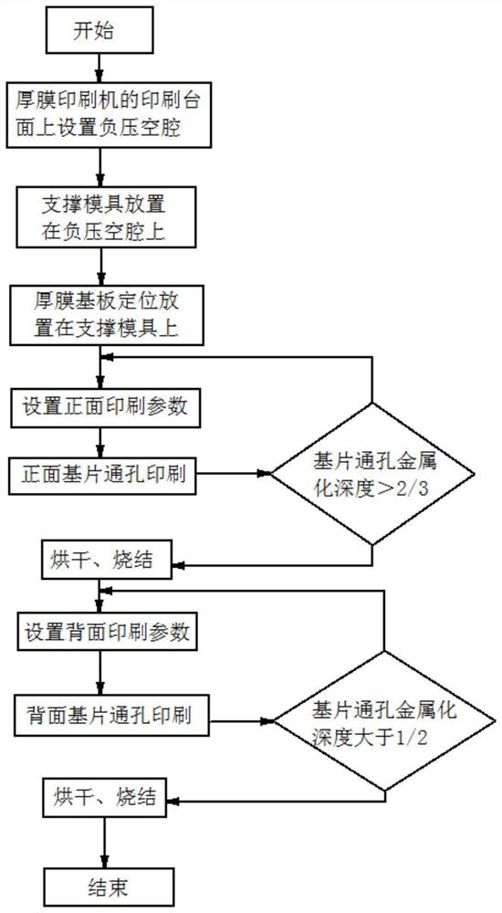
[0047] Step 1, Renovation of Printing Mesa 1:

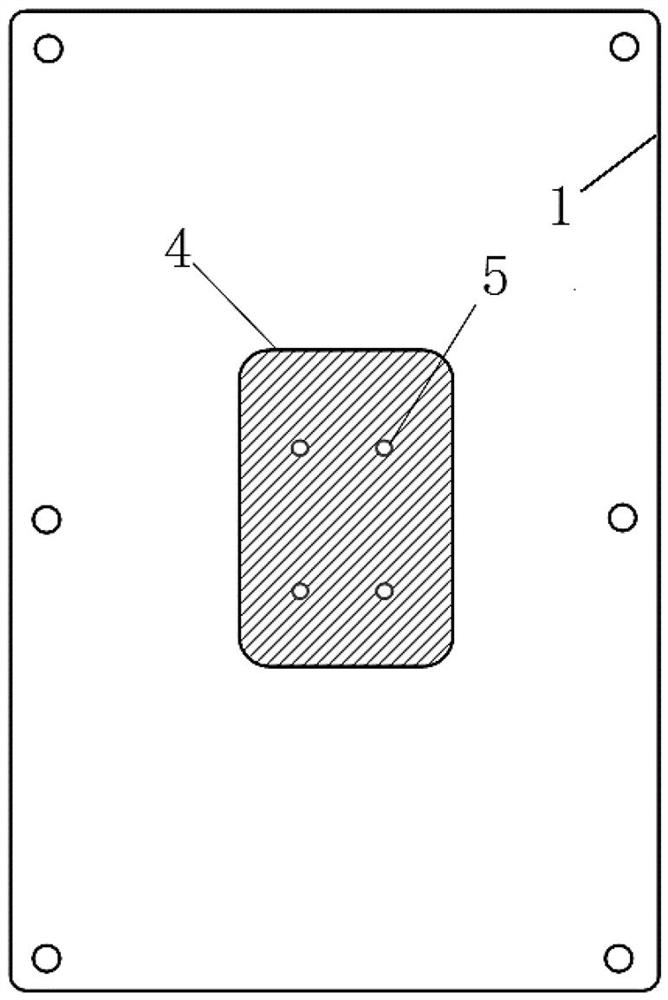
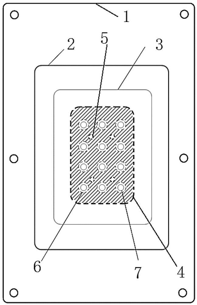
[0048] The air holes of the printing table of the ordinary printing machine can only be used for substrate positioning in the printing process. The printing table 1 of the thick film printing machine is modified, and a negative pressure chamber 4 of 50mm×50mm×2mm is made in the middle area of ​​the printing table 1. A cavity is formed below the film substrate 3, and the cavity structure consists of figure 1 with figure 2 As shown, it is beneficial to the gas flow in the negative pressure channel, so that the slurry forms adhesion on the side wall of the through hole of the substrate.

[0049] Step 2, production of supporting mold:

[0050] The support mold 2 corresponding to the thick film substrate 3 is fixed above the negative pressure chamber 4, so that the cavity for the adsorption of the substrate through hole 7 of the thick film substrate 3 is completed, and the support mold 2 is also used as the thick film substrate 3 s...


PUM

PropertyMeasurementUnit
thicknessaaaaaaaaaa

Abstract

The invention provides a method for realizing interconnection of front and back surface patterns of a thick film substrate. Interconnection through holes can be manufactured through a common printing machine, through hole interconnection is achieved while the patterns on the front surface and the back surface of the thick film substrate are manufactured, and the production efficiency can be improved. According to the invention, the substrate through holes on the front and back surfaces of the thick film substrate are respectively printed; and the interconnection of the metalized positive and negative lines on the side wall of the substrate through holes is consolidated, and the interconnectivity between the metalized positive and negative lines on the side wall of the substrate through holes is improved. Meanwhile, a process platform is built for manufacturing other through hole interconnection substrates, the method can be quickly and effectively popularized to other products by replacing a supporting mold, and good practicability and an economic value are achieved.

Description

technical field [0001] The invention relates to the technical field of high-density hybrid integrated circuits, in particular to an interconnection method for realizing front and back patterns of a thick-film substrate. Background technique [0002] With the development of high-density hybrid integrated circuits, the demand for wiring and interconnection on the front and back sides of thick film ceramic substrates is increasing. At present, the reliability of the front and back interconnections is limited, and the use of ordinary thick film printers to produce such substrates is abnormal Difficulties, so that the side walls of the through holes of the thick-film ceramic substrate cannot be interconnected normally, and the requirements for graphic interconnection on the front and back sides of the substrate cannot be realized without damaging the strength of the substrate. The method involved in this patent can well solve this problem. a question. Contents of the invention ...

Claims


Application Information

Patent Timeline
Patent Type & Authority Applications(China)
IPC IPC(8): H01L21/48B41M1/12B41M1/34
CPCH01L21/486B41M1/12B41M1/34
Inventor 吴鑫李创袁海任英哲魏震张泽于慧游
Owner XIAN MICROELECTRONICS TECH INST
Why Eureka
Try Eureka