Semiconductor structure and forming method thereof

A semiconductor and conformal technology, applied in semiconductor devices, microstructure technology, microstructure devices, etc., can solve the problem of easily increasing the difficulty of MEMS device process, achieve the improvement of interconnection capability, raise the interconnection surface, and reduce the difficulty of the process Effect

Pending Publication Date: 2022-04-15
NINGBO SEMICON INT CORP
View PDF0 Cites 0 Cited by
  • Summary
  • Abstract
  • Description
  • Claims
  • Application Information

AI Technical Summary

Problems solved by technology

[0004] In view of this, the present application provides a semiconductor structure and its formation method to solve the problem that traditional interconnection schemes tend to increase the difficulty of the MEMS device process

Method used


Image

  • Semiconductor structure and forming method thereof
  • Semiconductor structure and forming method thereof
  • Semiconductor structure and forming method thereof

Examples


Embodiment Construction

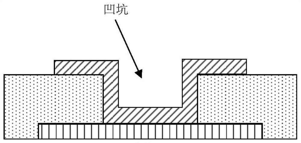
[0045] In sensing MEMS devices or optical MEMS devices, such as microactuators, the interconnection between semiconductor structures usually uses interconnection processes such as metal interconnection. It is an important process, and its process characteristics have an important impact on the subsequent process of the integrated circuit and the performance of the resulting circuit. In the traditional interconnection process, in order to ensure the interconnection between the two conductive layers, it is usually necessary to set a via hole with a larger size. The vias interconnect the second-level metal with the first-level metal. The via hole with the above-mentioned larger size will appear as follows after the second conductive layer is filled. figure 1 If the pits shown are used directly for subsequent interconnection, the pits will have too many turns, which will affect the difficulty of subsequent interconnection processes. If the pit is filled, the pit will require sub...


PUM


Abstract

The invention discloses a semiconductor structure and a forming method thereof, and the method comprises the steps: providing a substrate, and forming a conductive region on the surface of the substrate; forming a first dielectric layer on the conductive region, wherein the first dielectric layer at least exposes part of the surface of the conductive region; a first conducting layer is formed on the surface of the first dielectric layer, and the first conducting layer covers the first dielectric layer in a shape-preserving mode and further covers the surface of the exposed conducting area; a second dielectric layer is formed on the substrate, the second dielectric layer covers the substrate and other surfaces except the top surface of the first conductive layer, and the surface of the second dielectric layer is flush with the top surface of the first conductive layer; and forming a second conductive layer on the second dielectric layer, wherein the second conductive layer at least covers part of the top surface of the first conductive layer. The difficulty of each subsequent process can be reduced; the whole top surface of the second conductive layer serves as a subsequent interconnection area, so that the interconnection area is increased, and the interconnection capability of the corresponding semiconductor structure is improved.

Description

technical field [0001] The present application relates to the technical field of integrated circuits, in particular to a semiconductor structure and a method for forming the same. Background technique [0002] MEMS (Micro Electromechanical System, micro electromechanical device) has developed rapidly in recent years. It is a technology for designing, processing, manufacturing, measuring and controlling micron and / or nanomaterials, including mechanical components, optical systems, drive components and electrical components. It is widely used in the fields of intelligent systems, consumer electronics, wearable devices, smart homes, synthetic biology of system biotechnology and microfluidic technology. MEMS devices are mainly divided into four categories, sensing MEMS devices, biological MEMS devices, optical MEMS devices and radio frequency MEMS devices. MEMS technology is developing into a huge industry. At present, the leading products in the MEMS market are micro-actuators...

Claims


Application Information

Patent Timeline
IPC IPC(8): B81C1/00B81B7/00
Inventor 韩凤芹李萍桂珞
Owner NINGBO SEMICON INT CORP
Why Eureka
Try Eureka