Method for manufacturing integrated circuit

A production method and technology of integrated circuits, which are applied in the manufacture of circuits, electrical components, semiconductors/solid-state devices, etc., can solve the problems of high process difficulty, increased difficulty of integrated circuits, and extremely high requirements for MOS tube precision control, so as to reduce the process Difficulty, improve process development and effect

Active Publication Date: 2014-01-01
FOUNDER MICROELECTRONICS INT
View PDF4 Cites 6 Cited by
  • Summary
  • Abstract
  • Description
  • Claims
  • Application Information

AI Technical Summary

Problems solved by technology

[0003] However, when the above-mentioned method is used to fabricate a double-polycrystalline integrated circuit, the process of fabricating the insulating dielectric layer of the double-polycrystalline capacitor and the upper plate of the double-polycrystalline capacitor will have an impact on the parameters and characteristics of the previously fabricated MOS transistors, so In actual production

Method used


Image

  • Method for manufacturing integrated circuit
  • Method for manufacturing integrated circuit
  • Method for manufacturing integrated circuit

Examples


Embodiment Construction

[0043] The following will clearly and completely describe the technical solutions in the embodiments of the present invention with reference to the accompanying drawings in the embodiments of the present invention. Obviously, the described embodiments are only some, not all, embodiments of the present invention. Based on the embodiments of the present invention, all other embodiments obtained by persons of ordinary skill in the art without creative efforts fall within the protection scope of the present invention.

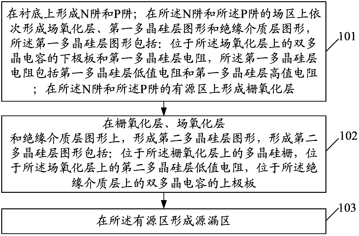
[0044] An embodiment of the present invention provides a method for manufacturing an integrated circuit, such as figure 1 As shown, the method includes:

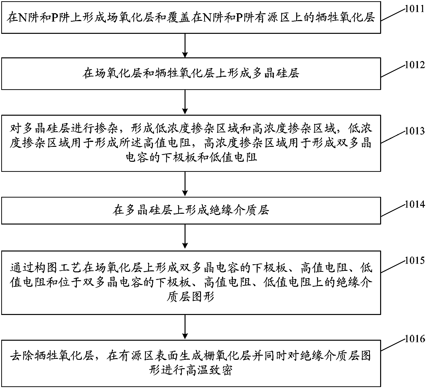
[0045] 101. Form an N well and a P well on the substrate; sequentially form a field oxide layer, a first polysilicon layer pattern, and an insulating dielectric layer pattern on the field regions of the N well and the P well, and the first The polysilicon layer pattern includes: the lower plate of the double pol...


PUM

PropertyMeasurementUnit
Thicknessaaaaaaaaaa

Abstract

The invention provides a method for manufacturing an integrated circuit and relates to the field of integrated circuit manufacture. The method can reduce the process difficulty and improve the flexibility of integrated circuit process development and integrated circuit design. The method for manufacturing an integrated circuit comprises the following steps: forming an N well and a P well on a substrate; sequentially forming a field oxide layer, a first polycrystalline silicon layer pattern and an insulating medium layer pattern respectively on field regions of the N well and the P well, wherein the first polycrystalline silicon layer pattern includes a lower electrode plate of a double polycrystalline silicon capacitor located on the field oxide layer, and a first polycrystalline silicon layer resistor; forming a gate oxide layer on active regions of the N well and the P well; forming a second polycrystalline silicon layer pattern on the gate oxide layer, the field oxide layer and the insulating medium layer pattern, wherein the second polycrystalline silicon layer pattern includes a polycrystalline silicon gate located on the gate oxide layer, a second polycrystalline silicon layer low-value resistor located on the field oxide layer, and an upper electrode plate of the double polycrystalline silicon capacitor located on the insulating medium layer; and forming a source and drain regions in the active regions.

Description

technical field [0001] The invention relates to the field of integrated circuit manufacturing, in particular to an integrated circuit manufacturing method. Background technique [0002] A dual polysilicon integrated circuit is an integrated circuit that contains components (such as dual polysilicon capacitors) composed of two layers of polysilicon. In the traditional preparation process of double polysilicon integrated circuits, the first layer of polysilicon is used to make the metal oxide semiconductor (Metal-Oxide-Semiconductor, MOS) tube in the integrated circuit and the lower plate of the double polysilicon capacitor, and then the double polysilicon is fabricated The insulating dielectric layer of the capacitor, and then use the second layer of polysilicon to make the upper plate of the double polycrystalline capacitor. [0003] However, when the above-mentioned method is used to fabricate a double-polycrystalline integrated circuit, the process of fabricating the insu...

Claims


Application Information

Patent Timeline
IPC IPC(8): H01L21/8234
CPCH01L21/823437H01L27/0629
Inventor 潘光燃
Owner FOUNDER MICROELECTRONICS INT
Why Eureka
Try Eureka