Glass passivation method for silicon mesa diodes

A mesa diode, glass passivation technology, applied in electrical components, semiconductor/solid-state device manufacturing, circuits, etc., can solve the problems of increasing production costs and high equipment requirements, achieving low dependence, good graphics quality, and reduced process difficulty. Effect

CN105470150AActive Publication Date: 2016-04-06NO 55 INST CHINA ELECTRONIC SCI & TECHNOLOGYGROUP CO LTD
10 Cites 6 Cited by

Patent Information

Authority / Receiving Office
CN · China
Current Assignee / Owner
Publication Date
2016-04-06

Smart Images

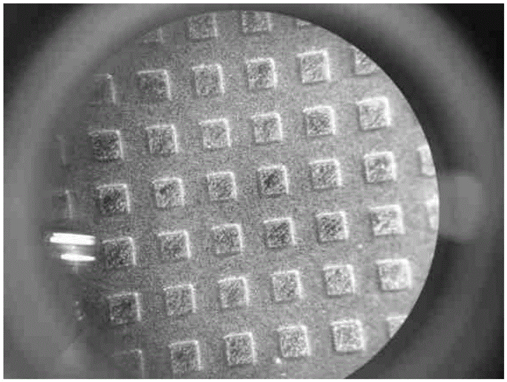
  • Figure 1
    Figure 1
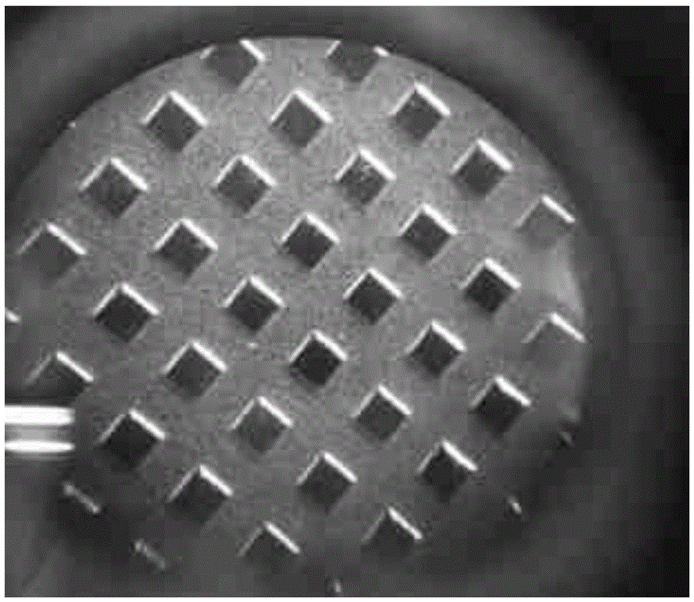
  • Figure 2
    Figure 2
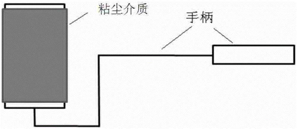
  • Figure 3
    Figure 3
Patent Text Reader

Abstract

The invention discloses a glass passivation method for silicon mesa diodes. The glass passivation method for silicon mesa diodes sequentially comprises the following steps: preparation of glass frit, glass coating, residual mesa top glass elimination, glass sintering and forming. The preparation proportion of the glass frit is optimized, mesa top glass is removed by an adhesion removal method, then a glass sintering process is carried out, difficulty of the process of eliminating the mesa top glass is reduced on the premise of achieving the ideal passivation effect, and the time of the process is shortened. According to a glass passivation device manufactured by the method, mesa top glass corrosion time can be shortened effectively, quality and precision of electrode window graphs are improved, the technology is simple and feasible, and production cost is reduced.
Need to check novelty before this filing date? Find Prior Art

Description

technical field

[0001] The invention belongs to the technical field of silicon device surface passivation, and in particular relates to a glass passivation method for silicon mesa diodes. Background technique

[0002] For silicon mesa diode devices, since the PN junction is exposed in the air, it is particularly sensitive to external influences, and surface contamination and surface charges will affect device parameters. The passivation film can passivate the active semiconductor Si surface, improve the performance of the device, strengthen the sealing of the device, shield the harmful effects of external impurities, ion charges, water vapor, etc. on the device, and enhance the stability and reliability of the device.

[0003] Glass passivation technology is a process in which passivation glass powder is coated on the surface of a silicon device, and the glass dielectric film is formed by heating and sintering. The dielectric film formed by glass passivation has a dense str...

Examples

Embodiment 1

[0041]In this embodiment, the glass passivation of silicon mesa diodes is carried out by referring to the above method. Wherein, the glass paste is prepared according to the following method: ethyl cellulose is added to the butyl carbitol solution in a ratio of 1g: 25ml, and after it is fully dissolved, it becomes a solvent for preparing the glass paste, and the paste solvent is mixed with the glass The powder was placed in an agate ball mill jar at a ratio of 1ml: 2g for ball milling, the ball milling speed was 220 rpm, and the ball milling time was 8 hours to obtain a glass slurry, which was then evenly coated with a stainless steel scraper with a flat knife edge. On the silicon wafer with PN junction and chip mesa groove, fill the mesa groove with glass paste, dry the above-mentioned wafer coated with glass paste with an infrared lamp, and place the wafer on a flat quartz plate , use a silica gel sticky roller to roll over the wafer evenly, and remove the glass powder on th...