MEMS wafer level vacuum packaging structure and method

A vacuum packaging and wafer-level technology, applied in the direction of microstructure technology, microstructure devices, processing microstructure devices, etc., can solve problems such as unstable bonding process and metal lead interconnection, so as to reduce process difficulty and improve reliability performance and yield, and the effect of ensuring airtightness

Inactive Publication Date: 2015-10-21
CHONGQING UNIV
View PDF6 Cites 6 Cited by
  • Summary
  • Abstract
  • Description
  • Claims
  • Application Information

AI Technical Summary

Problems solved by technology

[0005] In view of this, the object of the present invention is to provide a MEMS wafer-level vacuum packaging structure and processing method, the present invention can solve the p

Method used


Image

  • MEMS wafer level vacuum packaging structure and method
  • MEMS wafer level vacuum packaging structure and method
  • MEMS wafer level vacuum packaging structure and method

Examples


Embodiment Construction

[0038] The present invention will be further described below in conjunction with the accompanying drawings, and the examples given are only used to explain the present invention, and are not intended to limit the scope of the present invention.

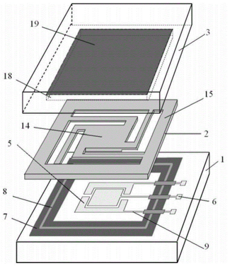
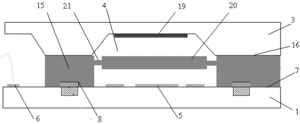
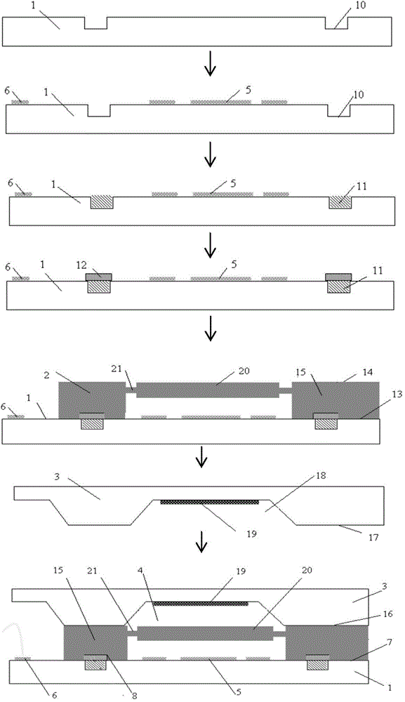
[0039] 1-insulating substrate; 2-MEMS chip structure layer; 3-cover plate; 4-vacuum chamber; 5-metal electrode; 6-pad; 7-first bonding ring; 8-second bonding ring; 9-metal lead; 10-groove I; 11-electric insulation layer; 12-bonding layer; 13-third bonding ring; 14-sensitive unit; 15-support structure; 16-fourth bonding ring; 17 - fifth bonding ring; 18 - groove II; 19 - film getter, 20 - sensitive mass; 21 - cantilever beam.

[0040] like figure 1 , figure 2 Shown is a three-dimensional view of the MEMS wafer-level vacuum packaging structure and a cross-sectional view of the MEMS wafer-level vacuum packaging structure of the present invention. The MEMS wafer-level vacuum packaging structure includes an insulating substrate 1, a MEM...


PUM

PropertyMeasurementUnit
Thicknessaaaaaaaaaa
Thicknessaaaaaaaaaa

Abstract

The invention discloses an MEMS wafer level vacuum packaging structure and method. The packaging structure comprises an insulation substrate, an MEMS chip structural layer and a cover plate, and the above components are connected through a wafer level bonding mode to form a vacuum cavity. The center of a first bonding ring is provided with a second bonding ring which is not totally closed, two types of bonding modes can be achieved in the same technical condition, because the bonding temperatures of anode bonding, gold and silicon eutectic bonding, hot pressing bonding or adhesion bonding are similar, so a vacuum packaging structure and metal wires can be transversally connected. In addition, the designed second bonding ring is slightly higher than the first bonding ring to make two bonding ring fully contact with each other during bonding, the second bonding ring is not totally closed, so on the one hand, metal wires can be transversally connected, and on the other hand, the vacuum cavity can be separated from the external environment, to make sure that the vacuum cavity is sealed. The MEMS wafer level vacuum packaging structure and method are simple in technology, the reliability and yield of device can be raised, and the application of MEMS wafer level vacuum packaging technology in a large scale scope can be promoted.

Description

technical field [0001] The invention belongs to the technical field of micro-electromechanical systems (MEMS) packaging, and in particular relates to a MEMS wafer-level vacuum packaging structure and a processing method. Background technique [0002] With the rapid development of micro-electromechanical systems (MEMS) technology, various MEMS device products have been used as high-quality sensors or detectors in the fields of industrial sensing, image communication, consumer electronics, automobile industry, military industry, etc. application. Many MEMS devices, such as micro-gyroscopes, micro-accelerometers, micro-filters, micro-ultrasonic sensors, and microbial molecular mass detectors based on resonant structures, need to be packaged in vacuum to reduce the gas damping of mechanical moving parts and improve the performance of the device. quality factor, thereby improving device performance. [0003] Vacuum packaging can be divided into device-level vacuum packaging and...

Claims


Application Information

Patent Timeline
IPC IPC(8): B81B7/00B81C1/00B81C3/00
Inventor 李东玲尚正国王胜强温志渝
Owner CHONGQING UNIV
Why Eureka
Try Eureka