Supercharge Your Innovation With Domain-Expert AI Agents!

Reverse blocking HEMT with stepped P-type GaN drain electrode structure

A reverse-resistance, step-type technology, applied in electrical components, circuits, semiconductor devices, etc., can solve the problems of uneven electric field distribution, unfavorable device reverse blocking voltage, increase, etc., to improve reverse breakdown voltage, The effect of uniform distribution of the electric field in the channel

Active Publication Date: 2021-11-12
UNIV OF ELECTRONIC SCI & TECH OF CHINA +1
View PDF9 Cites 3 Cited by
  • Summary
  • Abstract
  • Description
  • Claims
  • Application Information

AI Technical Summary

Problems solved by technology

The structure of the Schottky metal drain is simple, and it has a small turn-on voltage in the forward conduction, but in the reverse withstand voltage, the electric field distribution under the drain Schottky metal is uneven, and it will be at the edge of the drain region. The formation of high electric field peaks is not conducive to the improvement of the reverse blocking voltage of the device

Method used


Image

  • Reverse blocking HEMT with stepped P-type GaN drain electrode structure
  • Reverse blocking HEMT with stepped P-type GaN drain electrode structure
  • Reverse blocking HEMT with stepped P-type GaN drain electrode structure

Examples


Embodiment Construction

[0015] The scheme of the present invention will be described in detail below in conjunction with the accompanying drawings.

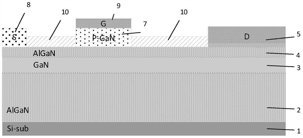
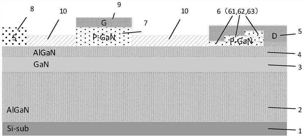
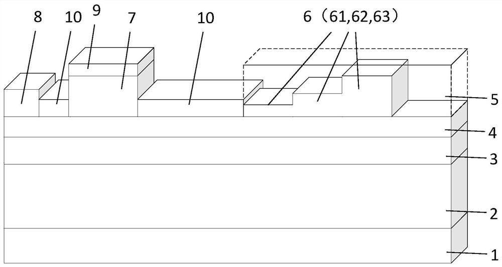
[0016] Such as figure 2 As shown, the device structure includes a substrate layer 1 from bottom to top, an AlGaN buffer layer 2, a GaN layer 3, and an AlGaN barrier layer 4, wherein the GaN layer and the AlGaN barrier layer form a heterojunction structure; in the AlGaN barrier layer One end of the active level metal 8 is connected to the gate P-type GaN material layer 7; the P-type GaN material layer 7 is connected to the gate metal 9 to realize an enhanced device; the upper part of the AlGaN barrier layer is covered by a passivation layer 10; At one end of the layer, a stepped P-type GaN material layer 6 is connected to the drain metal 5 to form a stepped P-type GaN drain structure, and the stepped P-type GaN material layer 6 is successively thinned in steps from the drain to the source.

[0017] The working principle of the reverse-resistance HEMT w...


PUM


Abstract

The invention relates to a power semiconductor technology, and especially relates to a reverse blocking HEMT with a stepped P-type GaN drain electrode structure. According to the invention, a P-type GaN layer in a drain electrode region is step-shaped, and is thinned in a step-type manner along the direction from the drain electrode to the source electrode. In the stepped P-type GaN drain electrode structure, each P-type GaN step is thinned in sequence in a stepped manner along the direction from the drain electrode to the source electrode, and the forward turn-on voltage at the thinner step is smaller during forward conduction, so that the turn-on voltage of the device is reduced. When the device is in a reverse blocking state, the channel electric field distribution of the drain region during reverse blocking is optimized through modulation of the stepped P-type GaN drain structure on the channel electric field, and the reverse blocking voltage of the device is improved. Compared with a traditional Schottky barrier drain reverse blocking type HEMT device, the reverse blocking voltage of the device is increased, and the channel electric field distribution of a drain region is optimized during reverse voltage withstanding.

Description

technical field [0001] The invention belongs to the technical field of power semiconductors, and relates to a reverse-resistance HEMT (High electron mobility transistor, high electron mobility transistor) with a stepped P-type GaN drain structure. Background technique [0002] With the development of contemporary society and technology, people have higher requirements for the utilization and management of electric energy. In terms of power conversion, power semiconductor technology plays a very important role. Nowadays, power semiconductor technology is closely related to people's daily life, which has greatly improved people's quality of life and level. The power semiconductor device is the foundation of power semiconductor technology, the core device of the power conversion system, and it is also a current research hotspot. As a third-generation wide-bandgap semiconductor material, gallium nitride (GaN) materials have high breakdown electric field strength, small dielect...

Claims


Application Information

Patent Timeline
IPC IPC(8): H01L29/778H01L29/06H01L29/08
CPCH01L29/7786H01L29/0619H01L29/0891
Inventor 孙瑞泽王茁成罗攀王方洲刘超陈万军
Owner UNIV OF ELECTRONIC SCI & TECH OF CHINA
Features
  • R&D
  • Intellectual Property
  • Life Sciences
  • Materials
  • Tech Scout
  • Unparalleled Data Quality
  • Higher Quality Content
  • 60% Fewer Hallucinations
Learn More