Method for automatically correcting electric leakage path of MOS device

A technology of MOS devices and correction methods, which is applied in the direction of instruments, electrical digital data processing, special data processing applications, etc., can solve the problems of not considering leakage path, unsatisfactory correction results, affecting production efficiency, etc., to solve time-consuming and error risks High, improve the level and quality of chip manufacturing, reduce the effect of manpower and time

Active Publication Date: 2021-11-16
SEMITRONIX
View PDF13 Cites 1 Cited by
  • Summary
  • Abstract
  • Description
  • Claims
  • Application Information

AI Technical Summary

Problems solved by technology

The common problem is: in a test structure, only the gate (gate) of the specific target device is connected to the signal, and the others are floating gate (floating gate). Since the voltage on the floating gate is not fixed, there is a certain The possibility of opening to a certain degree will increase the leakage path (leakage path) of the S / D terminal (source / drain terminal) of the target device, and the corresponding Ioff (off-state current) current value will be too large, which will affect the real electrical properties of the device. Analysis of characteristics
However, for MOS devices at present, the existence of such a leakage path is generally not considered, that is to say, no special attention has been paid to the impact of such a leakage path on the accurate measurement of the electrical characteristics of MOS devices.
Even if you pay attention to the problems caused by the leakage path, you can only rely on manual corrections based on subjective experience. The low correction efficiency also affects the overall production efficiency, and the correction results are not ideal and unstable.

Method used


Image

  • Method for automatically correcting electric leakage path of MOS device
  • Method for automatically correcting electric leakage path of MOS device
  • Method for automatically correcting electric leakage path of MOS device

Examples


Embodiment 1

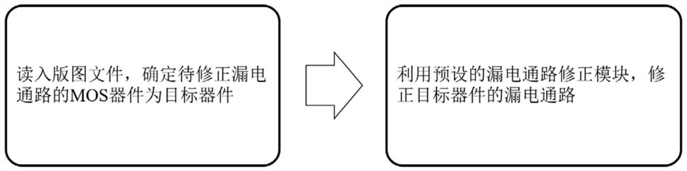
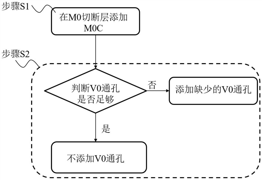
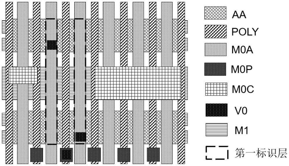
[0026] Such as figure 1 As shown, this embodiment provides a method for automatically correcting the leakage path of a MOS device, including: reading in the layout file, and determining the MOS device to be corrected as the target device; using the preset leakage path correction module to correct the target device Leakage path: In the leakage path correction module, the correction method of the MOS device with leakage path is defined. The correction method of this embodiment is as follows figure 2 As shown, step S1. Add M0C in the M0 cut-off layer, and cut off the M0 connection line to disconnect the source and / or drain of the target device from the source and of other MOS devices (ie floating gate, floating gate) / or the connection of the drain end; step S2. judge whether the source end, the drain end and the gate end of the target device can be respectively connected to the M1 connection line through the existing V0 through hole; if not, then add the missing V0 through hol...

Embodiment 2

[0035] In this embodiment, after the layout file is read in, the method of determining the MOS device to be corrected as the target device is given as an example, as shown in Figure 5 As shown, in step 1. Obtain the MOS device information in the layout file read in; Step 2. Use the preset leakage path screening module to screen whether there is a leakage path in the MOS device; Step 3. Screen the existence of the leakage path The MOS device is used as the target device.

[0036] The preset leakage path screening module defines conditions for judging whether there is a leakage path in the MOS device. The judgment conditions defined in this embodiment include: if there is a source terminal and a drain terminal of a certain MOS device connected together with source terminals and drain terminals of other MOS devices, it is judged that the MOS device is a MOS device with a leakage path; If the source terminal or drain terminal of a certain MOS device is connected to the source te...


PUM


Abstract

The invention provides a method for automatically correcting an electric leakage path of an MOS device. The method comprises the following steps of: reading a layout file, and automatically correcting by utilizing a preset electric leakage path correction module; and defining a correction mode of the MOS device with the electric leakage path in the electric leakage path correction module: adding an M0C to an M0 cut-off layer, and adding a lacked V0 through hole. The problem that the electrical property test of the MOS device is influenced by generation of an electric leakage path is effectively solved, and the authenticity of the electrical property test of the device is improved; and the method is simple in steps, does not depend on manual operation and experience, saves manpower and working hours, reduces the process research and development cost, solves the problems that manual correction is time-consuming and the error risk is high, is better in reliability of an automatic correction result, and facilitates the improvement of the manufacturing level and the overall quality of a product.

Description

technical field [0001] The invention belongs to the technical field of semiconductor design and manufacture, and in particular relates to a method for automatically correcting leakage paths of MOS devices. Background technique [0002] In the semiconductor industry, whether the chip can work normally is of great concern. From the perspective of circuit composition, the chip is composed of devices, and the electrical characteristics of the device itself are crucial to the entire chip. The electrical characteristics of the device can be preliminarily obtained through simulation, and the simulation (Simulation) data is obtained through simulation; the device is measured after the chip is produced, and the test (Silicon) data is obtained. Compare simulated data with test data (S2S). By comparison, verify the accuracy of the simulation data and assist in judging the correctness of the test data. If the simulation data can accurately reflect the real electrical characteristics o...

Claims


Application Information

Patent Timeline
Patent Type & Authority Applications(China)
IPC IPC(8): G06F30/398
CPCG06F30/398
Inventor 王莹雪方益
Owner SEMITRONIX
Why Eureka
Try Eureka