CSP lamp bead packaging structure and manufacturing process thereof

A technology of packaging structure and manufacturing process, which is applied in the direction of electrical components, circuits, semiconductor devices, etc., can solve the problems that the process temperature cannot be approached or exceeded, the secondary melting of the die-bonding solder, and the small adhesion, etc., to improve the small welding area , increase the weldable area, improve the effect of welding adhesion

Pending Publication Date: 2021-11-16
ZHONGSHAN MULINSEN ELECTRONICS CO LTD
View PDF0 Cites 0 Cited by
  • Summary
  • Abstract
  • Description
  • Claims
  • Application Information

AI Technical Summary

Problems solved by technology

[0003] figure 1 The obvious disadvantages of the CSP of structure 1 are that the pads are small, the effective welding area of ​​CSP is small, the adhesion is small, and the reliability and production yield of the back-end products are low.
figure 2 The effective soldering area of ​​the CSP of structure 2 is relatively large, but it uses die-bonding solder to electrically connect the electrodes of the LED chip 1 and the bracket 5. The obvious disadvantage is that the process temperature in the latter stage cannot approach or exceed the temperature of the die-bonding solder. Otherwise, there will be a problem of secondary melting of the die-bonding solder

Method used


Image

  • CSP lamp bead packaging structure and manufacturing process thereof
  • CSP lamp bead packaging structure and manufacturing process thereof
  • CSP lamp bead packaging structure and manufacturing process thereof

Examples


Embodiment 1

[0053] Such as Figure 3-13As shown, a manufacturing process of a CSP lamp bead packaging structure includes the following steps:

[0054] S1. Cutting and bonding: prepare the metal substrate 31 of the metal layer 3 and the insulating substrate 21 of the insulating carrier layer 2 with suitable sizes, and bond the materials of the metal substrate 31 and the insulating substrate 21 together;

[0055] S2. Making circuits and opening holes: making a preset metal pattern on the metal substrate 31, and opening holes on the insulating substrate;

[0056] S3. Arranging crystals: arranging the LED chips 1 in the openings, and forming a distance between the electrodes 10 of the LED chips 1 and the metal substrate 31;

[0057] S4. Film pressing: Press the prepared fluorescent adhesive film from the top of the chip, and package the LED chip 1, insulating substrate 21 and metal substrate 31 to form a fluorescent adhesive layer. The fluorescent adhesive 4 is on the LED chip 1. filling th...

Embodiment 2

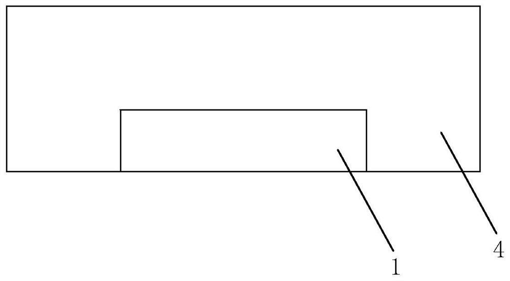
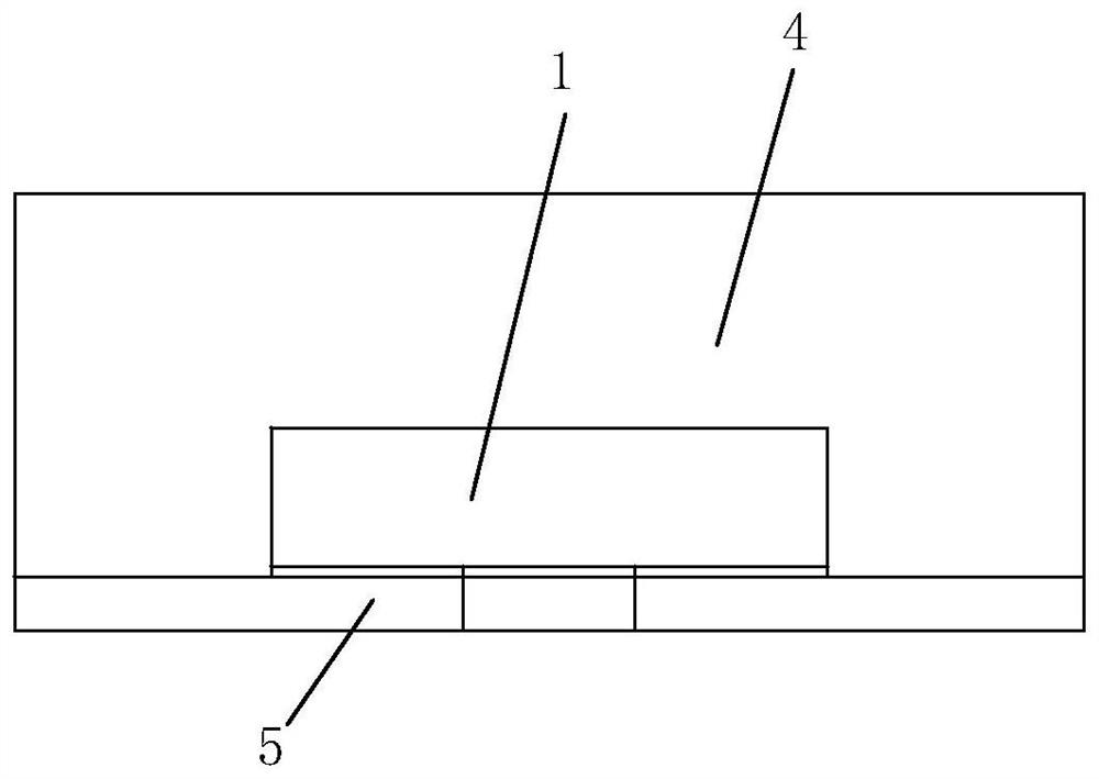
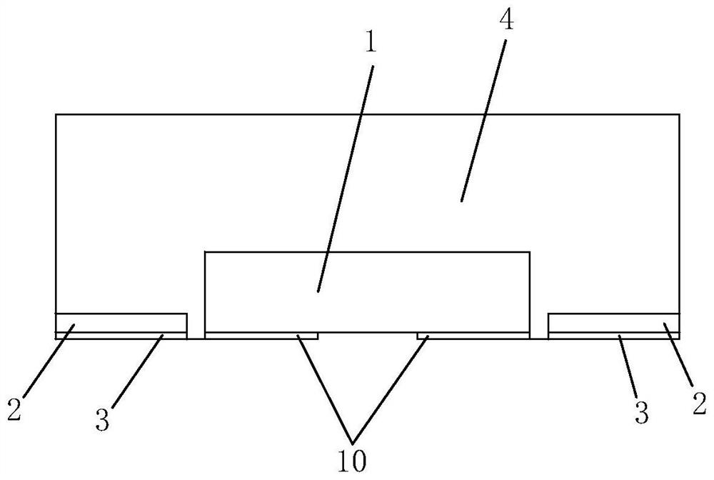
[0081] Such as Figure 3-13 As shown, a CSP lamp bead packaging structure includes LED chip 1, insulating carrier layer 2, metal layer 3 and fluorescent glue 4; electrode 10 is provided at the bottom of LED chip 1; insulating carrier layer 2 is arranged around said LED chip 1 side; the metal layer 3 is arranged at the bottom of the insulating carrier layer 2, and has a distance from the electrode 10; the fluorescent glue 4 encapsulates the LED chip 1, the insulating carrier layer 2 and the metal layer 3, and makes the electrode 10. The bottom surface and the bottom surface of the metal layer 3 are exposed. An insulating carrier layer is arranged around the LED chip, and a metal layer with a distance from the electrode of the LED chip is arranged at the bottom of the insulating carrier layer. The LED chip and the insulating carrier layer are bonded together by fluorescent glue. Packaged with the metal layer, this application sets the metal layer at intervals on the side of the ...


PUM

PropertyMeasurementUnit
Thicknessaaaaaaaaaa
Thicknessaaaaaaaaaa
Thicknessaaaaaaaaaa

Abstract

The invention provides a CSP lamp bead packaging structure and a manufacturing process thereof. A metal base material and an insulating base material are attached, then a preset metal base material pattern is manufactured on the metal base material, then an opening for loading an LED chip is formed in the insulating base material, the LED chip is arranged in the opening, a gap is formed between an electrode of the LED chip and the metal base material, the LED chip, the insulation base material and the metal base material are packaged through a fluorescent glue film, the surface of the bottom of the electrode of the LED chip and the surface of the bottom of the metal base material are exposed, and finally the single CSP lamp bead packaging structure is formed through cutting. The metal layer is arranged on the electrode side of the LED chip at an interval, the metal layer serves as the extension bonding pad of the electrode of the LED chip, the weldable area of the CSP is increased, in addition, no solid crystal welding flux exists, the problem of secondary fusion of the CSP solid crystal welding flux caused by too high temperature of the rear section can be effectively avoided, the temperature limitation of the rear-end product is solved, and the method is suitable for the complex process of multiple reflow soldering.

Description

technical field [0001] The application belongs to the technical field of LED packaging, and in particular relates to a CSP lamp bead packaging structure and a manufacturing process thereof. Background technique [0002] CSP (Chip Scale Package) LED has attracted much attention and favor for its high reliability and small size. Common CSP structures generally have two structures, such as figure 1 Structure 1 shown: includes LED chip 1, fluorescent glue 4; as figure 2 The second structure shown: includes bracket 5 , die-bonding solder, LED chip 1 and fluorescent glue 4 . [0003] figure 1 The obvious disadvantages of the CSP of structure 1 are that the pads are small, the effective welding area of ​​CSP is small, the adhesion is small, and the reliability and production yield of the back-end products are low. figure 2 The effective soldering area of ​​the CSP of structure 2 is relatively large, but it uses die-bonding solder to electrically connect the electrodes of the ...

Claims


Application Information

Patent Timeline
IPC IPC(8): H01L33/38H01L33/52
CPCH01L33/385H01L33/387H01L33/52
Inventor 皮保清王洪贯石红丽
Owner ZHONGSHAN MULINSEN ELECTRONICS CO LTD
Why Eureka
Try Eureka