High-voltage CSP lamp bead packaging structure and manufacturing process thereof

A technology of packaging structure and manufacturing process, which is applied in the direction of electrical components, electrical solid devices, circuits, etc., can solve the problems of easy secondary melting, small pads, and unsuitability for use in high-voltage environments, and improve the effective welding area. , increase the weldable area, and release the effect of temperature limitation

Pending Publication Date: 2022-03-25
ZHONGSHAN MULINSEN ELECTRONICS CO LTD
View PDF0 Cites 0 Cited by
  • Summary
  • Abstract
  • Description
  • Claims
  • Application Information

AI Technical Summary

Problems solved by technology

[0005] The first purpose of the present invention is to provide a manufacturing process of high-voltage CSP lamp bead packaging structure in order to solve the technical problems of the traditional CSP structure with small pads, easy secondary melting and unsuitability for use in high-voltage environments

Method used


Image

  • High-voltage CSP lamp bead packaging structure and manufacturing process thereof
  • High-voltage CSP lamp bead packaging structure and manufacturing process thereof
  • High-voltage CSP lamp bead packaging structure and manufacturing process thereof

Examples


Embodiment 1

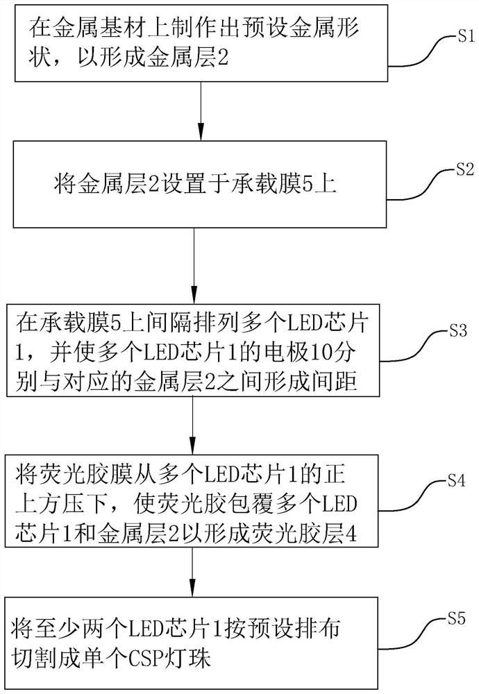
[0062] Such as Figure 4-11 As shown, a manufacturing process of a high-voltage CSP lamp bead packaging structure includes the following steps:

[0063] S1. Make a preset metal pattern on the metal substrate, clean and leave the metal layer 2 required for this application;

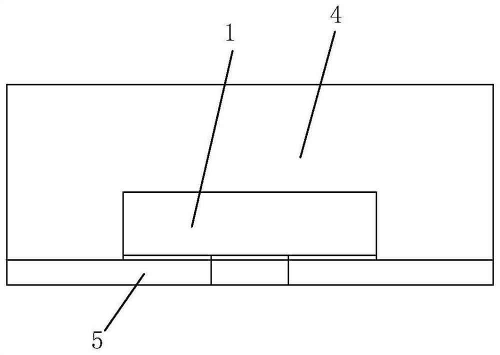
[0064] S2, disposing the metal layer 2 on the carrier film 5;

[0065] S3, arranging a plurality of LED chips 1 at intervals on the carrier film 5, and forming a distance between the electrodes 10 of the plurality of LED chips 1 and the corresponding metal layer 2;

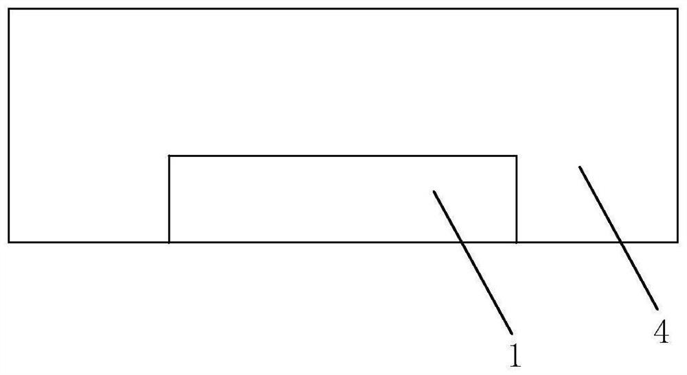
[0066] S4. Press the fluorescent adhesive film from directly above the plurality of LED chips 1, make the fluorescent adhesive cover the plurality of LED chips 1 and the metal layer 2 to form the fluorescent adhesive layer 4, and make the bottom surface of the electrode 10 of the LED chip 1 and the bottom surface of the LED chip 1 The bottom surface of the metal layer 2 is exposed;

[0067] S5. Cutting at least two LED chips 1 into a single...

Embodiment 2

[0072] Such as Figure 12-19 As shown, a manufacturing process of a high-voltage CSP lamp bead packaging structure includes the following steps:

[0073] S1. Make a preset metal pattern on the metal substrate, clean and leave the metal layer 2 required for this application;

[0074] S2, disposing the metal layer 2 on the carrier film 5;

[0075] S3, arranging a plurality of LED chips 1 at intervals on the carrier film 5, and forming a distance between the electrodes 10 of the plurality of LED chips 1 and the corresponding metal layer 2;

[0076] S4. Press the fluorescent adhesive film from directly above the plurality of LED chips 1, make the fluorescent adhesive cover the plurality of LED chips 1 and the metal layer 2 to form the fluorescent adhesive layer 4, and make the bottom surface of the electrode 10 of the LED chip 1 and the bottom surface of the LED chip 1 The bottom surface of the metal layer 2 is exposed;

[0077] S5. Cutting at least two LED chips 1 into a singl...

Embodiment 3

[0082] Such as Figure 20-28 As shown, a manufacturing process of a high-voltage CSP lamp bead packaging structure includes the following steps:

[0083] S1. Make a preset metal pattern on the metal substrate, clean and leave the metal layer 2 required for this application;

[0084] S2, disposing the metal layer 2 on the carrier film 5;

[0085] S3, arranging a plurality of LED chips 1 at intervals on the carrier film 5, and forming a distance between the electrodes 10 of the plurality of LED chips 1 and the corresponding metal layer 2;

[0086] S4. Set up a retaining wall 3 around the side of the LED chip 1 through glue dispensing, film pressing or injection molding process;

[0087] S5. Press the fluorescent adhesive film from directly above the plurality of LED chips 1, make the fluorescent adhesive cover the plurality of LED chips 1, the metal layer 2 and the retaining wall 3 to form the fluorescent adhesive layer 4, and make the electrodes of the LED chips 1 10 the bot...


PUM

PropertyMeasurementUnit
thicknessaaaaaaaaaa

Abstract

The invention provides a high-voltage CSP lamp bead packaging structure and a manufacturing process thereof, the high-voltage CSP lamp bead packaging structure comprises a plurality of LED chips which are arranged at intervals, metal layers which are arranged at the peripheral sides of the electrodes of the LED chips at intervals, and fluorescent glue layers which are used for packaging the LED chips and the metal layers, the design of the plurality of LED chips enables a product of the scheme to form a high-voltage CSP after the product is pasted on a substrate, current can be uniformly diffused, and the quality of the product is improved. According to the invention, direct high-voltage driving is realized, the applicability is wider, the metal layers are arranged on the electrode side of the LED chip at intervals, so that the metal layers can serve as extended bonding pads of the LED chip electrode, the weldable area of the CSP is increased, the problem that the effective welding area of an existing CSP packaging structure is small can be effectively solved, the welding adhesive force of the CSP and the reliability and the production yield of a CSP rear-end product are improved, and the production cost is reduced. Meanwhile, the CSP packaging structure is free of solid crystal welding flux, the problem of secondary fusion of the CSP solid crystal welding flux caused by too high temperature of the rear section can be effectively avoided, the temperature limitation of the rear-end product is solved, and the CSP packaging structure is suitable for the complex process of multiple reflow soldering.

Description

technical field [0001] The application belongs to the technical field of LED lamp bead packaging, and in particular relates to a high-voltage CSP lamp bead packaging structure and a manufacturing process thereof. Background technique [0002] CSP (Chip Scale Package) LED has attracted much attention and favor for its high reliability and small size. Common CSP structures generally have two structures, such as figure 2 Structure 1 shown: includes LED chip 1, fluorescent adhesive layer 4; as image 3 The second structure shown: includes bracket 5 , die-bonding solder, LED chip 1 , fluorescent adhesive layer 4 . [0003] figure 2 The obvious disadvantages of the CSP of structure 1 are that the pads are small, the effective welding area of ​​CSP is small, the adhesion is small, and the reliability and production yield of the back-end products are low. image 3 The effective welding area of ​​the CSP of the second structure is relatively large, but it uses die-bonding solder ...

Claims


Application Information

Patent Timeline
Patent Type & Authority Applications(China)
IPC IPC(8): H01L25/075H01L33/50H01L33/52H01L33/62
CPCH01L25/0753H01L33/505H01L33/62H01L33/52H01L2933/0066H01L2933/0033
Inventor 皮保清王洪贯罗德伟石红丽
Owner ZHONGSHAN MULINSEN ELECTRONICS CO LTD
Why Eureka
Try Eureka