
Nitride device and preparation method thereof

A nitride and device technology, applied in the field of nitride devices and its preparation, can solve problems such as chip function failure and damage to integrated circuits

Pending Publication Date: 2021-11-23
XIAMEN SANAN INTEGRATED CIRCUIT
View PDF0 Cites 0 Cited by
  • Summary
  • Abstract
  • Description
  • Claims
  • Application Information

AI Technical Summary

Problems solved by technology

When the external environment of the chip or the inside of the chip accumulates a certain amount of static electricity, when it flows into or out of the chip through the pins of the chip, the instantaneous current (peak value can reach several amperes) or voltage will damage the integrated circuit, causing Chip function failure

Method used


Image

  • Nitride device and preparation method thereof
  • Nitride device and preparation method thereof
  • Nitride device and preparation method thereof

Examples


Embodiment Construction

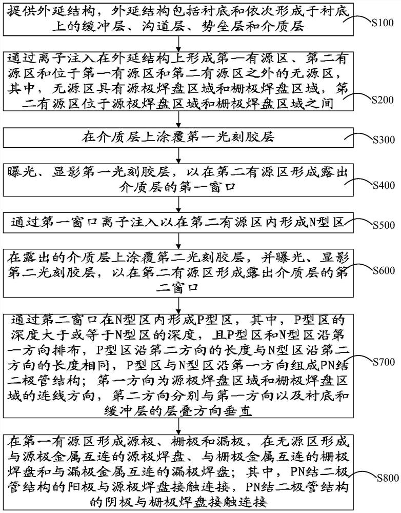
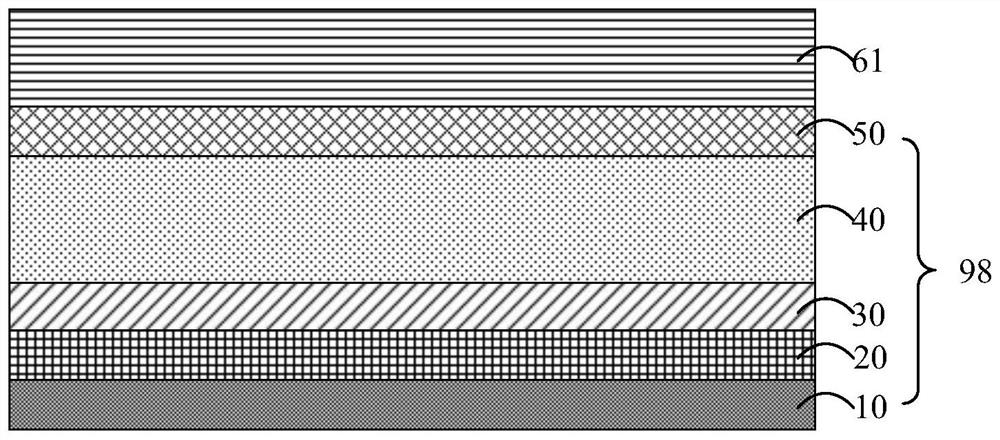
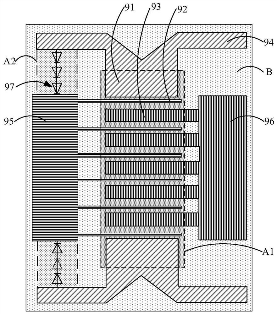
[0030] The embodiments set forth below represent the information necessary to enable one skilled in the art to practice the embodiments and illustrate the best mode of practicing the embodiments. Upon reading the following description with reference to the accompanying drawing figures, those skilled in the art will understand the concepts of the disclosure and will recognize applications of these concepts not specifically addressed herein. It should be understood that these concepts and applications are within the scope of this disclosure and the appended claims.

[0031] It will be understood that, although the terms first, second, etc. may be used herein to describe various elements, these elements should not be limited by these terms. These terms are only used to distinguish one element from another. For example, a first element could be termed a second element, and, similarly, a second element could be termed a first element, without departing from the scope of the presen...


PUM

PropertyMeasurementUnit
Doping concentrationaaaaaaaaaa

Abstract

The invention discloses a nitride device and a preparation method thereof, and relates to the technical field of semiconductor devices. The preparation method comprises the following steps: providing an epitaxial structure; forming a first active region, a second active region and a passive region on the epitaxial structure through ion implantation; forming a first window for exposing the dielectric layer of the epitaxial structure in the second active region through a photoetching process; performing ion implantation through the first window to form an N-type region in the second active region; forming a second window for exposing the dielectric layer in the second active region through a photoetching process; forming a P-type region in the N-type region through the second window, and the P-type region and the N-type region being connected in series to form a PN junction diode structure; forming a source electrode, a grid electrode and a drain electrode in the first active region, and forming a source electrode bonding pad, a grid electrode bonding pad and a drain electrode bonding pad in the passive region; wherein the anode of the PN junction diode structure is in contact connection with the source electrode bonding pad, and the cathode of the PN junction diode structure is in contact connection with the grid electrode bonding pad. The preparation method can improve the tolerance level of the reverse voltage between the grid electrode and the source electrode of the device.

Description

technical field [0001] The present disclosure relates to the technical field of semiconductor devices, in particular, to a nitride device and a preparation method thereof. Background technique [0002] Electro-Static discharge (ESD) is a phenomenon of charge release and transfer between integrated circuit chips and external objects. When the external environment of the chip or the inside of the chip accumulates a certain amount of static electricity, when it flows into or out of the chip through the pins of the chip, the instantaneous current (peak value can reach several amperes) or voltage will damage the integrated circuit, causing The chip function fails. With the development of the semiconductor industry, the feature size is further reduced, the density of components is increasing, and the possibility of electronic components being damaged by static electricity is also increasing. In order to avoid damage to integrated circuits caused by static electricity, the electro...

Claims


Application Information

Patent Timeline
IPC IPC(8): H01L29/20H01L29/78H01L21/336H01L27/02
CPCH01L29/2003H01L29/7818H01L29/66522H01L27/0255
Inventor 蔡文必刘胜厚卢益锋孙希国谷鹏其他发明人请求不公开姓名
Owner XIAMEN SANAN INTEGRATED CIRCUIT
Learn More