Planar diode chip capable of preventing silver migration

A diode and planar technology, applied in the field of planar diode chips, can solve problems such as anode and cathode short circuits, and achieve the effects of avoiding lateral migration, facilitating chip processing, and good solderability

Pending Publication Date: 2021-11-26
LESHAN RADIO
View PDF0 Cites 0 Cited by
  • Summary
  • Abstract
  • Description
  • Claims
  • Application Information

AI Technical Summary

Problems solved by technology

[0004] The purpose of the present invention is to provide a planar diode for the problem that silver ions in the first metal layer migrate to both sid

Method used


Image

  • Planar diode chip capable of preventing silver migration
  • Planar diode chip capable of preventing silver migration
  • Planar diode chip capable of preventing silver migration

Examples


Embodiment 1

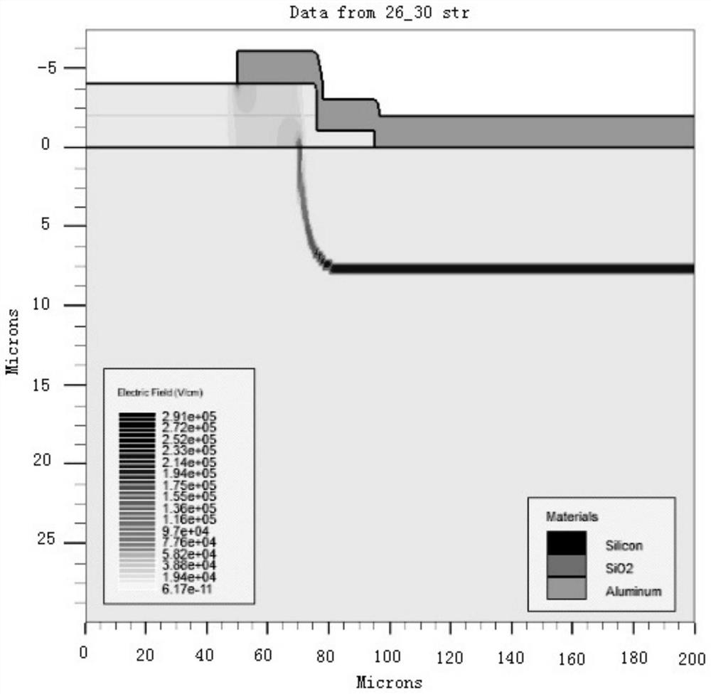
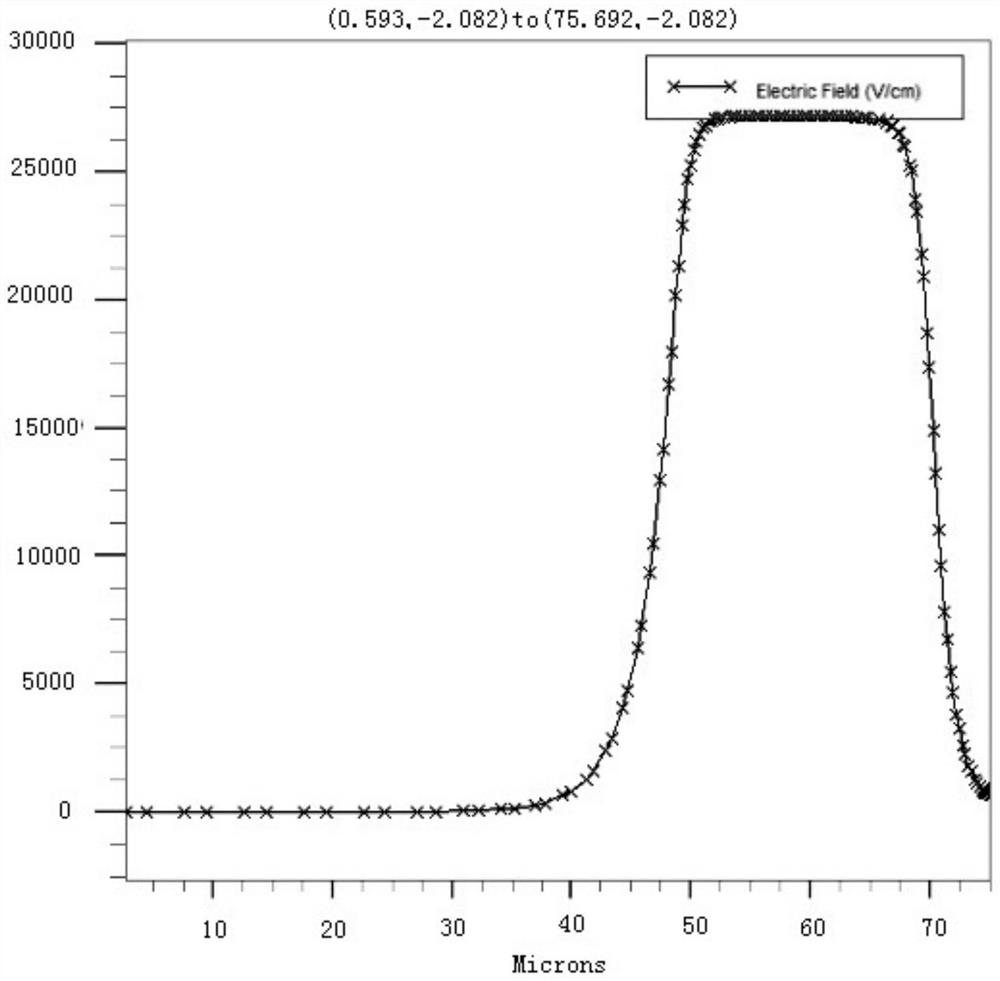
[0037] A planar diode chip, such as Figure 4 As shown, including a first semiconductor layer 1, a second semiconductor layer 2 disposed on the surface of the first semiconductor layer 1, the first semiconductor layer 1 and the second semiconductor layer 2 provide a diode structure; in the second semiconductor layer 2 The outer surface of the first semiconductor layer 1 is provided with a protective layer 3 for protecting the PN junction;

[0038] A first metal layer is provided on the surface of the second semiconductor layer 2 away from the first semiconductor layer 1 ; the first metal layer includes a soldering layer 4 , and the soldering layer 4 is located in the middle of the second semiconductor layer 2 .

[0039] The first metal layer further includes a conductive layer 5 , and the conductive layer 5 is located between the soldering layer 4 and the second semiconductor layer 2 . The conductive layer 5 is a metal that is less prone to ionization than silver. The conduc...

Embodiment 2

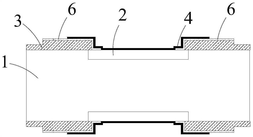
[0047] This embodiment is a 79mil planar TVS chip, based on the structure of Embodiment 1, an insulating layer 6 is provided between the second metal layer and the protective layer 3 . Such as Figure 5 As shown, the first semiconductor layer 1 is P-type, and the second semiconductor layer 2 and the third semiconductor layer are respectively arranged on the upper and lower sides of the first semiconductor layer 1, and both the second semiconductor layer 2 and the third semiconductor layer are N + type. The surface of the second semiconductor layer 2 is provided with a first metal layer, the surface of the third semiconductor layer is provided with a second metal layer, and the first metal layer and the third metal layer are mirror images.

[0048] side profile Figure 5 In the first metal layer on the upper side as an example, the N + The upper side of the second semiconductor layer 2 is provided with a Ti / Al conductive layer 5, and the conductive layer 5 covers the second ...

Embodiment 3

[0051] The difference between this embodiment and Embodiment 1 lies in that, in the first metal layer, the conductive layer 5 and the soldering layer 4 are arranged differently. Such as Figure 9 As shown, the first metal layer further includes a conductive layer 5 , and the conductive layer 5 is located on the surface of the second semiconductor layer 2 on the outer periphery of the soldering layer 4 . The solder layer 4 is in direct contact with the surface of the second semiconductor layer 2 .


PUM


Abstract

The invention relates to a planar diode chip, in particular to a planar diode chip capable of preventing silver migration, which comprises a first semiconductor layer and a second semiconductor layer arranged on the surface of the first semiconductor layer, and the first semiconductor layer and the second semiconductor layer provide a diode structure; a protection layer for protecting a PN junction is arranged on the surface of the first semiconductor layer on the periphery of the second semiconductor layer; a first metal layer is arranged on the surface, far away from the first semiconductor layer, of the second semiconductor layer; the first metal layer comprises a welding layer, and the welding layer is located in the middle of the second semiconductor layer. The transverse electric fields at the two ends of the welding layer and the two ends of the semiconductor layer are spaced, so that the influence of the transverse electric fields is reduced; meanwhile, the distance from the surface of the welding layer to the side surface of the chip is increased, the possibility of forming a conductive moisture film between the silver electrode and the side surface electrode of the chip is reduced, and the risk of silver migration on the surface of the planar diode chip can be reduced.

Description

technical field [0001] The invention relates to a planar diode chip, in particular to a planar diode chip preventing silver migration. Background technique [0002] Diode chips in planar technology, such as figure 1 As shown, it includes the first semiconductor layer, the second conductivity type region and the protective layer for protecting the PN junction from bottom to top. A first metal layer is provided on the upper surface of the second conductivity type region, and the first metal layer usually adopts Ti / Ni / Ag. In cross section, the width of the first metal layer is greater than the width of the first semiconductor layer, such as figure 1 Among them, the first metal layer exceeds the first semiconductor layer to the left and right sides respectively. [0003] Since the first metal layer straddles the first semiconductor layer and the protective layer is close to the first semiconductor layer, there is a lateral electric field, and the ionized silver ions can easil...

Claims


Application Information

Patent Timeline
IPC IPC(8): H01L23/482H01L29/861
CPCH01L23/4824H01L23/4827H01L29/8611
Inventor 邱志述谭志伟陈鹏
Owner LESHAN RADIO
Why Eureka
Try Eureka