Camera module and manufacturing method thereof

The technology of a camera module and manufacturing method is applied in the direction of image communication, TV, color TV parts, etc., which can solve the problems of unfavorable image sensor chip heat dissipation and unfavorable thinning of camera module, so as to improve the heat dissipation effect and reduce the The effect of thickness, thin thickness

Active Publication Date: 2021-11-26
HONGQISHENG PRECISION ELECTRONICS (QINHUANGDAO) CO LTD +1
View PDF5 Cites 0 Cited by
  • Summary
  • Abstract
  • Description
  • Claims
  • Application Information

AI Technical Summary

Problems solved by technology

But this is not conducive to the thinning of the camera module and the heat dissipation of the image sensing chip.

Method used


Image

  • Camera module and manufacturing method thereof
  • Camera module and manufacturing method thereof
  • Camera module and manufacturing method thereof

Examples


Embodiment Construction

[0058] The following will clearly and completely describe the technical solutions in the embodiments of the present invention with reference to the accompanying drawings in the embodiments of the present invention. Obviously, the described embodiments are only some, not all, embodiments of the present invention. Based on the embodiments of the present invention, all other embodiments obtained by persons of ordinary skill in the art without making creative efforts belong to the protection scope of the present invention.

[0059] Unless otherwise defined, all technical and scientific terms used herein have the same meaning as commonly understood by one of ordinary skill in the technical field of the invention. The terms used herein in the description of the present invention are for the purpose of describing specific embodiments only, and are not intended to limit the present invention.

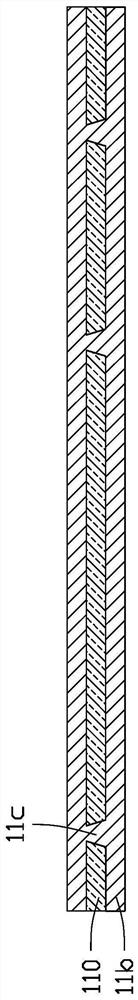
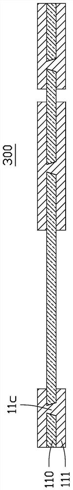
[0060] An embodiment of the present invention provides a method for manufacturing a camera ...


PUM


Abstract

The invention relates to a manufacturing method of a camera module, which comprises the following steps of: providing a circuit board, and forming a through slot in the circuit board; providing a reinforcing plate made of heat conduction material and having a groove, the groove being provided with a bottom and a side wall surrounding the bottom; arranging the reinforcing plate on one side of the circuit board and enabling the groove to correspond to the slot, wherein the groove communicates with the slot to form a containing space; installing an image sensor in the containing space and electrically connecting the image sensor with an image sensing chip and the circuit board, wherein the image sensing chip is in contact with the bottom and the side wall of the groove; and providing an optical lens, and arranging the optical lens on one side, opposite to the reinforcing plate, of the circuit board to obtain the camera module. In addition, the invention also provides a camera module.

Description

technical field [0001] The invention relates to a camera module and a manufacturing method thereof. Background technique [0002] With the accelerated development of full-screen mobile phones, the camera module must not only meet the camera function, but also be thin and short. The packaging structure of the image sensor chip is one of the important factors affecting the size of the image camera module. [0003] In the prior art, the photosensitive chip is usually installed on one side of the circuit board, and then the bracket with the lens and the filter is installed on the same side of the circuit board, so that the photosensitive chip is accommodated in the bracket and opposite to the filter. However, this is not conducive to the thinning of the camera module and the heat dissipation of the image sensing chip. Contents of the invention [0004] In view of this, it is necessary to provide a camera module which is thin and easy to dissipate heat. [0005] In addition, ...

Claims


Application Information

Patent Timeline
Patent Type & Authority Applications(China)
IPC IPC(8): H04N5/225
CPCH04N23/52H04N23/54H04N23/50
Inventor 彭满芝刘瑞武
Owner HONGQISHENG PRECISION ELECTRONICS (QINHUANGDAO) CO LTD
Why Eureka
Try Eureka