

Flexible PCB defect detection method, visual system, device and medium
A PCB board and defect detection technology, applied in the field of image processing, can solve the problems of defect sample classification, high cost, and low intelligence, and achieve high-speed defect sample identification, labor cost saving, and high progress.
- Summary
- Abstract
- Description
- Claims
- Application Information
AI Technical Summary
Problems solved by technology
Method used
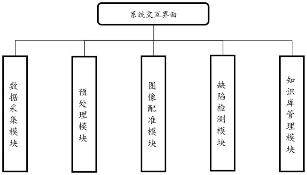
Image

Examples
Embodiment Construction
[0051] Embodiments of the present invention are described in detail below, and examples of the embodiments are shown in the drawings, wherein the same or similar reference numerals denote the same or similar elements or elements having the same or similar functions throughout. The embodiments described below by referring to the figures are exemplary only for explaining the present invention and should not be construed as limiting the present invention. For the step numbers in the following embodiments, it is only set for the convenience of illustration and description, and the order between the steps is not limited in any way. The execution order of each step in the embodiments can be adapted according to the understanding of those skilled in the art sexual adjustment.
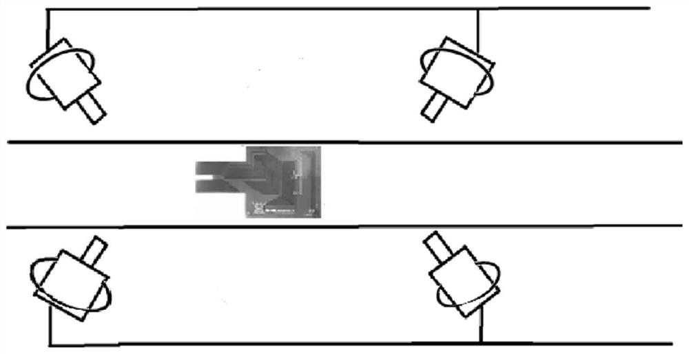
[0052]The automatic optical inspection system must improve the resolution of the camera to completely obtain the sample image on the assembly line, so as to obtain more complete information of the flexible PCB...
PUM
 Abstract
Description
Claims
Application Information