
Fin morphology design method in FinFET structure

A design method and morphology technology, applied in the field of Fin morphology design, can solve the problems of not being able to meet the anti-penetration risk at the bottom of high-mobility FIN at the same time, and achieve the effect of narrowing the width and improving the short channel effect

Pending Publication Date: 2021-12-10
SHANGHAI HUALI INTEGRATED CIRCUTE MFG CO LTD
View PDF0 Cites 0 Cited by
  • Summary
  • Abstract
  • Description
  • Claims
  • Application Information

AI Technical Summary

Problems solved by technology

[0005] In view of the above-mentioned shortcomings of the prior art, the purpose of the present invention is to provide a method for designing the Fin morphology in the FinFET structure, which is used to solve the problem that the channel at the bottom of the FIN cannot be simultaneously satisfied in the prior art during the manufacturing process of the FinFET structure. Problems with high mobility and the risk of penetration resistance at the bottom of the FIN

Method used


Image

  • Fin morphology design method in FinFET structure
  • Fin morphology design method in FinFET structure
  • Fin morphology design method in FinFET structure

Examples


Embodiment Construction

[0030] Embodiments of the present invention are described below through specific examples, and those skilled in the art can easily understand other advantages and effects of the present invention from the content disclosed in this specification. The present invention can also be implemented or applied through other different specific implementation modes, and various modifications or changes can be made to the details in this specification based on different viewpoints and applications without departing from the spirit of the present invention.

[0031] see Figure 2 to Figure 8 . It should be noted that the diagrams provided in this embodiment are only schematically illustrating the basic idea of ​​the present invention, and only the components related to the present invention are shown in the diagrams rather than the number, shape and shape of the components in actual implementation. Dimensional drawing, the type, quantity and proportion of each component can be changed arb...


PUM


Abstract

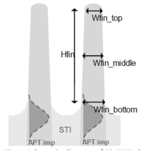
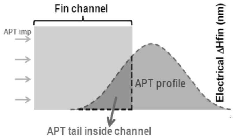
The invention provides a Fin morphology design method in a FinFET structure. A plurality of Fin structures located on a substrate, the Fin structures, buffer layers on the Fin structures and hard mask layers on the Fin structures form a lamination layer; the side wall of the lamination layer is covered with a first side wall; an organic distribution layer is deposited, and etching is conducted until a part of the side wall of the Fin structure is exposed; an organic distribution layer is continuously deposited to partially wrap the Fin structure; a second side wall is formed on the side wall of the lamination layer; the organic distribution layer is completely removed, and the side wall part, which makes contact with the organic distribution layer, of the Fin structure is exposed; an oxide layer is deposited by using an FCVD method, and annealing is conducted, wherein the width of the exposed Fin structure is narrowed due to oxidation in the annealing process; and etching is conducted to remove the hard mask layer, the buffer layer and the second side wall. According to the invention, part of the Fin structure used as an NMOS and a PMOS is oxidized through FCVD to reduce the width of the Fin structure, the anti-punch-through region with the narrowed width is obtained, and less doping or no doping can be used for the part of the anti-punch-through region. By reducing the width of the anti-punch-through region, a better short channel effect can be obtained.

Description

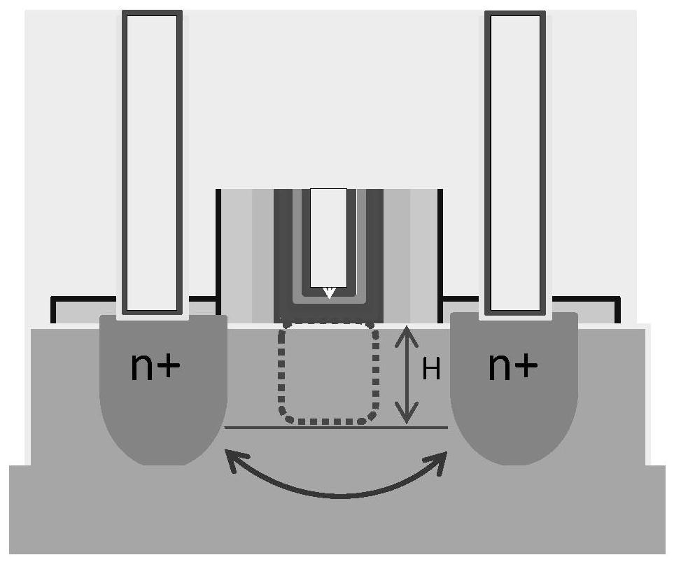
technical field [0001] The invention relates to the technical field of semiconductors, in particular to a method for designing Fin morphology in a FinFET structure. Background technique [0002] With the continuous expansion of MOS scale, FinFET (fin transistor) devices have become a further technical expansion of CMOS. The main advantage of the FinFET device structure is its superior electrostatic integrity, which is largely dependent on the channel morphology. Figure 1a Shown as a schematic diagram of a FinFET structure in the prior art, where the FIN (fin portion) is wrapped by a metal gate (MG) below the depth H of the top of the FIN, and the lower part of the FIN has a greater risk of penetration, especially when the source and drain The deeper the channel, the higher the doping concentration. [0003] At present, after APT (anti-punch through) doping implantation, there is a problem of damage. The top doping concentration of FIN is extremely low, and the mobility of c...

Claims


Application Information

Patent Timeline
Patent Type & Authority Applications(China)
IPC IPC(8): H01L21/336
CPCH01L29/66795
Inventor 李勇
Owner SHANGHAI HUALI INTEGRATED CIRCUTE MFG CO LTD
Learn More