N-type silicon carbide single crystal wafer stripping method and stripping device

A silicon carbide single crystal, silicon carbide technology, applied in chemical instruments and methods, single crystal growth, single crystal growth and other directions, can solve the problems of poor peeling method and other problems, and achieve the effect of low cost and simple operation

Active Publication Date: 2022-01-07
ZHEJIANG UNIV HANGZHOU GLOBAL SCI & TECH INNOVATION CENT
View PDF4 Cites 4 Cited by
  • Summary
  • Abstract
  • Description
  • Claims
  • Application Information

AI Technical Summary

Problems solved by technology

[0004] The purpose of the present invention is to overcome the problem of poor effect of existing strippi

Method used


Image

  • N-type silicon carbide single crystal wafer stripping method and stripping device
  • N-type silicon carbide single crystal wafer stripping method and stripping device
  • N-type silicon carbide single crystal wafer stripping method and stripping device

Examples


Embodiment Construction

[0031] The following will clearly and completely describe the technical solutions in the embodiments of the present invention with reference to the accompanying drawings in the embodiments of the present invention. Obviously, the described embodiments are only some, not all, embodiments of the present invention. Based on the embodiments of the present invention, all other embodiments obtained by persons of ordinary skill in the art without making creative efforts belong to the protection scope of the present invention.

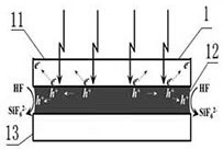
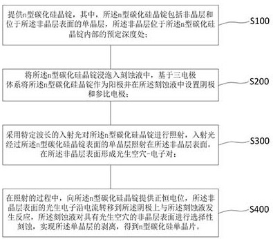
[0032] see figure 1 , the present embodiment provides a technical solution: a method for peeling off an n-type silicon carbide single wafer, comprising the following steps:

[0033] Step S100: Provide an n-type silicon carbide ingot, wherein the n-type silicon carbide ingot includes an amorphous layer and a single crystal layer located on the surface of the amorphous layer, and the amorphous layer is located on the n-type silicon carbide at a predetermined de...


PUM


Abstract

The invention relates to the field of silicon carbide single crystal wafer manufacturing, and discloses an n-type silicon carbide single crystal wafer stripping method and stripping device. The n-type silicon carbide single crystal wafer stripping method comprises the steps of providing an n-type silicon carbide crystal ingot comprising an amorphous layer and a single crystal layer located on the surface of the amorphous layer; soaking the n-type silicon carbide crystal ingot into an etching solution, taking the n-type silicon carbide crystal ingot as an anode based on a three-electrode system, and arranging a cathode and a reference electrode in the etching solution; irradiating the n-type silicon carbide crystal ingot by using incident light with a specific wavelength, wherein the incident light irradiates the surface of the amorphous layer to form a photo-generated hole-electron pair; and in the irradiation process, providing positive constant potential for the n-type silicon carbide crystal ingot, so as to enable photo-induced electrons on the surface of the amorphous layer to be transferred to a cathode along current to react with etching liquid, and the etching liquid to selectively etch the surface of the amorphous layer, and further to achieve stripping of the single crystal layer and obtain the n-type silicon carbide single crystal wafer. The surface or subsurface of the single crystal wafer obtained by the method has no damage layer and no stress residue, and is simple to operate and low in cost.

Description

technical field [0001] The invention relates to the technical field of single wafer manufacturing, in particular to an n-type silicon carbide single wafer peeling method and a peeling device. Background technique [0002] At present, in the silicon carbide ingot slicing process, the "laser cutting method" is a new method of producing silicon carbide single wafers, which is expected to replace the traditional "diamond wire cutting method". In a dry environment, the laser is focused on the cutting surface parallel to the basal plane of the silicon carbide ingot, and local heating generates high-density dislocations, forming a thin layer of amorphous silicon, An amorphous layer of amorphous carbon and amorphous silicon carbide, wherein the thickness of the amorphous layer is about 50 μm; and then a silicon carbide single wafer is obtained by mechanically peeling off the amorphous layer. [0003] The method has less dicing loss and fewer processing traces on the surface or subs...

Claims


Application Information

Patent Timeline
IPC IPC(8): C30B33/10C30B29/36C30B33/00
CPCC30B33/10C30B33/00C30B29/36
Inventor 耿文浩王蓉皮孝东王明华杨德仁
Owner ZHEJIANG UNIV HANGZHOU GLOBAL SCI & TECH INNOVATION CENT
Why Eureka
Try Eureka