Method for preparing QLED device, QLED device and display device
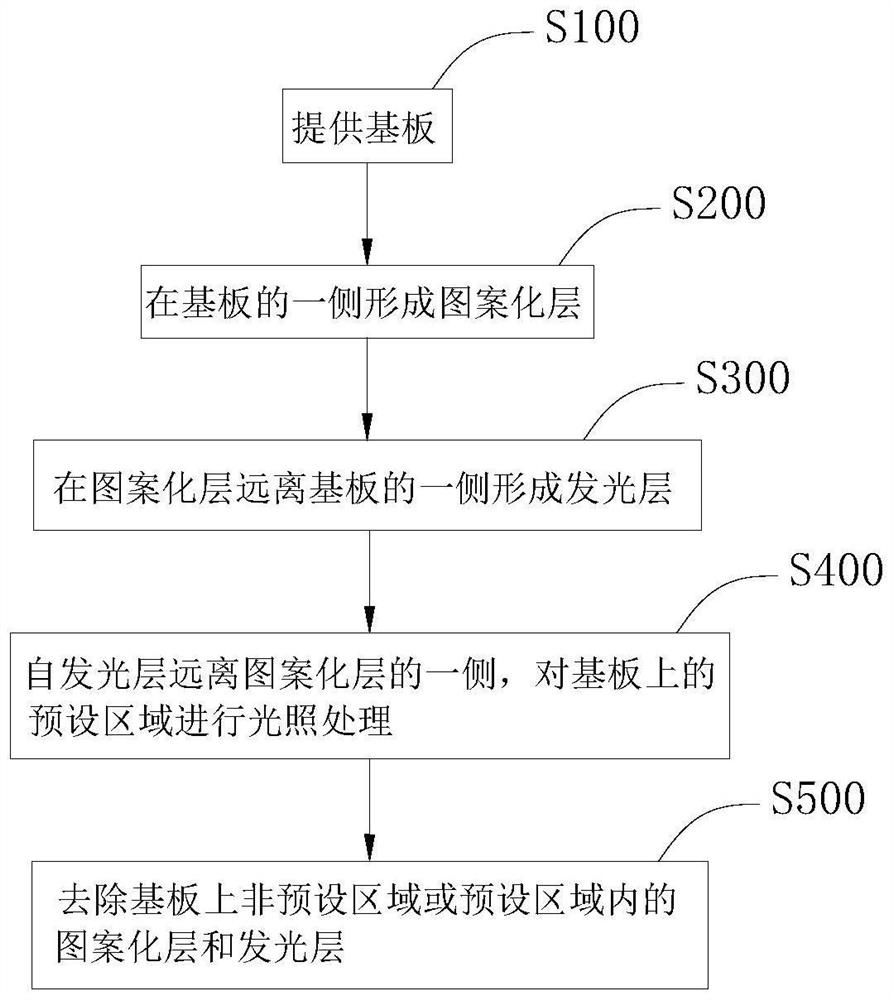
A device and patterned layer technology, applied in the field of QLED devices and display devices, can solve the problems that QLED devices and display devices need to be improved
- Summary
- Abstract
- Description
- Claims
- Application Information
AI Technical Summary
Problems solved by technology
Method used
Image
Examples
experiment example 1
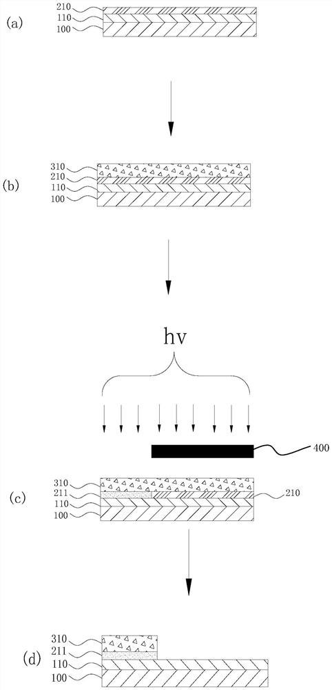
[0139] 1. The cathode is formed on the substrate, the substrate is conductive glass, and the material for forming the cathode is ITO.
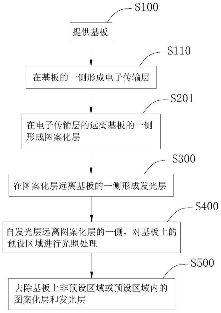
[0140] 2. An electron transport layer is formed on the side with the cathode on the substrate, and the material for forming the electron transport layer is zinc oxide nanoparticles. Specifically, 100 microliters of 20 mg / mL zinc oxide nanoparticles are dropped onto the above substrate, Set the speed of the homogenizer to 1500rpm and spin coat to form a film.
[0141] 3. Preparation of red QLED devices includes:
[0142] The first patterned layer is formed on the side of the electron transport layer away from the substrate, and the structural formula of the material forming the first patterned layer is as formula (1)
[0143]
[0144] The first color light-emitting layer is formed on the side of the first patterned layer away from the substrate. Specifically, the first color is red, and the material forming the first color light-emitting la...
experiment example 2
[0153] 1. The cathode is formed on the substrate, the substrate is conductive glass, and the material for forming the cathode is ITO.
[0154] 2. An electron transport layer is formed on the side with the cathode on the substrate. The material forming the electron transport layer is zinc oxide sol-gel. Specifically, 2g of zinc acetate is added to a mixed solvent containing 10mL of ethanolamine and 10mL of n-butanol, Spin coating to form a film at a speed of 3000 rpm, and heat on a hot stage at 200°C to form a film.
[0155] 3. Preparation of red QLED devices includes:
[0156] The fourth patterned layer is formed on the side of the electron transport layer away from the substrate, and the material structure formula of the fourth patterned layer is as formula (2)
[0157]
[0158] A fourth color light-emitting layer is formed on the side of the fourth patterned layer away from the substrate. Specifically, the fourth color is red, and the material forming the fourth color li...
PUM
| Property | Measurement | Unit |
|---|---|---|
| wavelength | aaaaa | aaaaa |
| wavelength | aaaaa | aaaaa |
Abstract
Description
Claims
Application Information
 - R&D Engineer
- R&D Manager
- IP Professional
- Industry Leading Data Capabilities
- Powerful AI technology
- Patent DNA Extraction
Browse by: Latest US Patents, China's latest patents, Technical Efficacy Thesaurus, Application Domain, Technology Topic, Popular Technical Reports.
© 2024 PatSnap. All rights reserved.Legal|Privacy policy|Modern Slavery Act Transparency Statement|Sitemap|About US| Contact US: help@patsnap.com


