Silicon wafer, cleaning method thereof and solar cell
A solar cell and cleaning technology, applied in the field of solar cells, can solve the problems of large loss of silicon wafers and difficult to control the degree of cleaning, and achieve the effect of reducing loss, ensuring quality, efficient and selective cleaning
- Summary
- Abstract
- Description
- Claims
- Application Information
AI Technical Summary
Problems solved by technology
Method used
Image

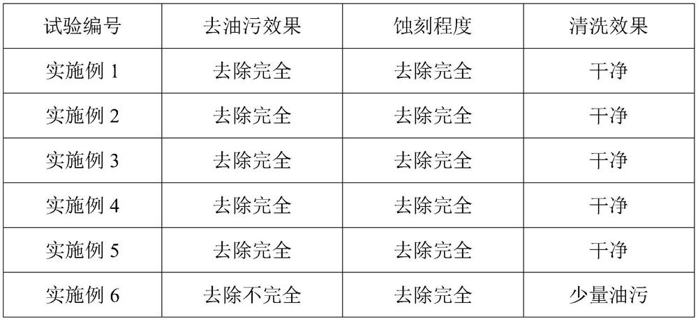
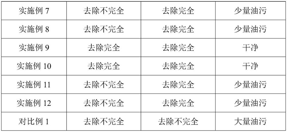
Examples
Embodiment 1
[0044] This embodiment provides a cleaning method for a silicon wafer, the cleaning method comprising the steps of:
[0045] (1) place the silicon chip with oil on the surface to oxidize in the air for 6 hours to obtain a silicon oxide chip;
[0046] (2) Pass into the mixed gas of carbon tetrafluoride and oxygen, step (1) gained silicon oxide chip is etched, the time is 750s, and temperature is 120 ℃, and the pressure of gas is 250Mpa, obtains etching silicon chip; The gas flow of fluorocarbon is 2500L / min, and the gas flow of said oxygen is 60L / min;
[0047] (3) Pickling the etched silicon wafer obtained in step (2) for 120 s with a mixed solution of hydrofluoric acid and hydrochloric acid, the pH range of the pickling solution is 4-6, and the cleaning of the silicon wafer is completed.
Embodiment 2
[0049] This embodiment provides a cleaning method for a silicon wafer, the cleaning method comprising the steps of:
[0050] (1) place the silicon chip with oil on the surface to oxidize in the air for 5 hours to obtain a silicon oxide chip;
[0051] (2) Feed a mixed gas of nitrogen trifluoride and oxygen, and etch the silicon oxide sheet obtained in step (1), the time is 600s, the temperature is 140°C, and the pressure of the gas is 300Mpa to obtain an etched silicon sheet; the three The gas flow of nitrogen fluoride is 2400L / min, and the gas flow of said oxygen is 50L / min;
[0052] (3) Pickling the etched silicon wafer obtained in step (2) with hydrofluoric acid for 100 s, the pH range of the pickling solution is 4-6, and the cleaning of the silicon wafer is completed.
Embodiment 3
[0054] This embodiment provides a cleaning method for a silicon wafer, the cleaning method comprising the steps of:
[0055] (1) place the silicon chip with oil on the surface to oxidize in the air for 7 hours to obtain a silicon oxide chip;
[0056] (2) Feed a mixed gas of trifluoromethane and oxygen, and etch the silicon oxide wafer obtained in step (1), the time is 800s, the temperature is 90°C, and the pressure of the gas is 200Mpa to obtain an etched silicon wafer; The gas flow of methane is 2500L / min, and the gas flow of said oxygen is 60L / min;
[0057] (3) Pickling the etched silicon wafer obtained in step (2) with hydrochloric acid for 140 s, the pH range of the pickling solution is 4-6, and the volume ratio of the mixed solution is to complete the cleaning of the silicon wafer.
PUM
 Abstract
Description
Claims
Application Information