Wafer back metallization method

A technology of backside metallization and wafer, which is applied in the direction of electrical components, semiconductor/solid-state device manufacturing, circuits, etc., can solve problems such as backgold peeling off at the edge of the dicing line, short circuit, and reduce the packaging yield of wafer backgold process, etc. To achieve the effect of improving yield rate and convenient deglue

Pending Publication Date: 2022-01-25
HYGON INFORMATION TECH CO LTD
View PDF0 Cites 1 Cited by
  • Summary
  • Abstract
  • Description
  • Claims
  • Application Information

AI Technical Summary

Problems solved by technology

[0003] However, the existing metallization process on the back of the wafer tends to cause the back gold on the edge of the dicing line to fall off during the cutting process, or the cut metal wire remains to cause short circuits in the packaging process, which reduces the cost of the wafer back gold process and subsequent packaging. Yield

Method used


Image

  • Wafer back metallization method
  • Wafer back metallization method
  • Wafer back metallization method

Examples


Embodiment Construction

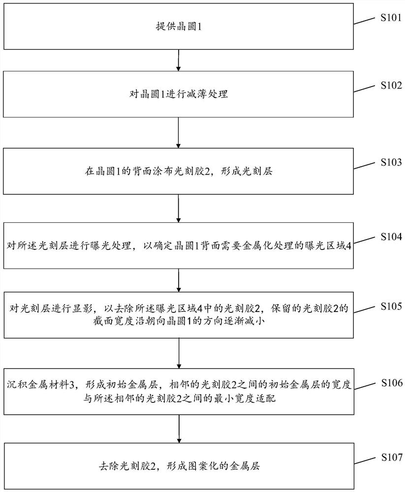
[0028] In order to make the purpose, technical solutions and advantages of the embodiments of the present invention clearer, the technical solutions in the embodiments of the present invention will be clearly and completely described below in conjunction with the drawings in the embodiments of the present invention. Obviously, the described embodiments It is only some embodiments of the present invention, but not all embodiments. Based on the embodiments of the present invention, all other embodiments obtained by persons of ordinary skill in the art without making creative efforts belong to the protection scope of the present invention.

[0029] It should be noted that in the present invention, relative terms such as first and second are only used to distinguish one entity or operation from another entity or operation, and do not necessarily require or imply that these entities or operations Any such actual relationship or order exists between. Furthermore, the term "comprise...


PUM


Abstract

The invention provides a wafer back metallization method. The method comprises the following steps of: providing a wafer; coating the back surface of the wafer with photoresist on to form a photoetching layer; performing exposure treatment on the photoetching layer to determine an exposure area needing metallization treatment on the back surface of the wafer; developing the photoetching layer to remove the photoresist in the exposure area, and making the section width of the reserved photoresist gradually reduced in the direction towards the wafer; depositing a metal material to form an initial metal layer, and enabling the width of the initial metal layer between adjacent photoresist to be matched with the minimum width between the adjacent photoresist; and removing the photoresist to form a patterned metal layer. According to the method of the invention, the yield of a wafer back gold process and subsequent packaging can be improved.

Description

technical field [0001] The invention relates to the technical field of chip packaging, in particular to a method for backside metallization of a wafer. Background technique [0002] With the increasing heat dissipation requirements of high-power devices and high-end chips, the application of backside metallization of wafers is also becoming more and more extensive. Backside metallization is a kind of physical vapor deposition (PVD). This process is a film preparation technology that deposits metal materials on the backside of the wafer by physical methods. After backside metallization, it can reduce the thermal resistance of the device and enhance the heat dissipation of the chip during operation. Capability; Individual power devices will lead out electrodes on the back, so that the die electrodes have good ohmic contact characteristics. [0003] However, the existing metallization process on the back of the wafer tends to cause the back gold on the edge of the dicing line ...

Claims


Application Information

Patent Timeline
Patent Type & Authority Applications(China)
IPC IPC(8): H01L21/02H01L21/027
CPCH01L21/02697H01L21/0274
Inventor 陈伯昌
Owner HYGON INFORMATION TECH CO LTD
Why Eureka
Try Eureka