PCB drilling defect detection device and detection method

A PCB board and defect detection technology, which is applied in measurement devices, workpiece clamping devices, optical testing defects/defects, etc., can solve the problems of difficult positioning and clamping, low efficiency, and non-adjustable acquisition height, and achieves improved clarity. , Easy to view, improve the effect of positioning and clamping efficiency

Inactive Publication Date: 2022-01-28
深圳市浩创盛科技股份有限公司
View PDF10 Cites 1 Cited by
  • Summary
  • Abstract
  • Description
  • Claims
  • Application Information

AI Technical Summary

Problems solved by technology

[0007] The purpose of the present invention is to provide a PCB board drilling defect detection device and detection method to solve the problems of difficult positioning and clamping, non-adjustable collection height and low efficiency in the above background technology

Method used


Image

  • PCB drilling defect detection device and detection method
  • PCB drilling defect detection device and detection method
  • PCB drilling defect detection device and detection method

Examples


Embodiment Construction

[0040] The following will clearly and completely describe the technical solutions in the embodiments of the present invention with reference to the accompanying drawings in the embodiments of the present invention. Obviously, the described embodiments are only some, not all, embodiments of the present invention. Based on the embodiments of the present invention, all other embodiments obtained by persons of ordinary skill in the art without making creative efforts belong to the protection scope of the present invention.

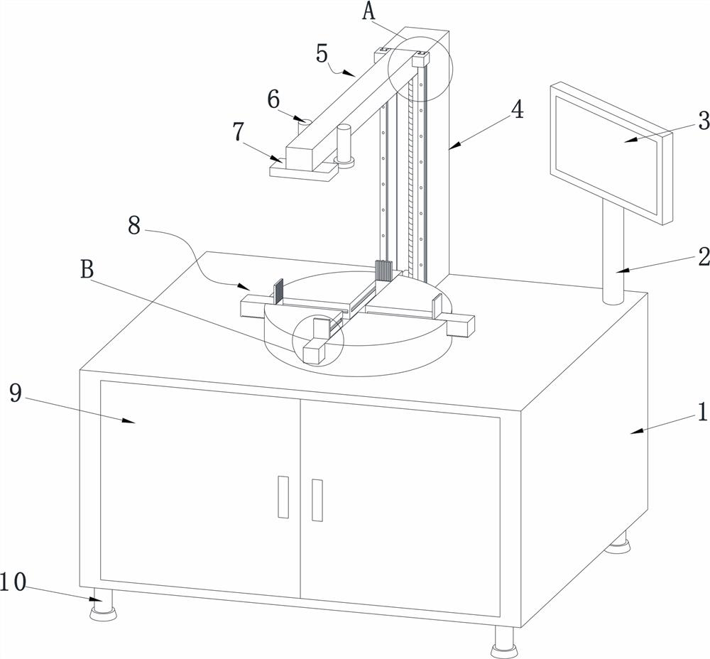
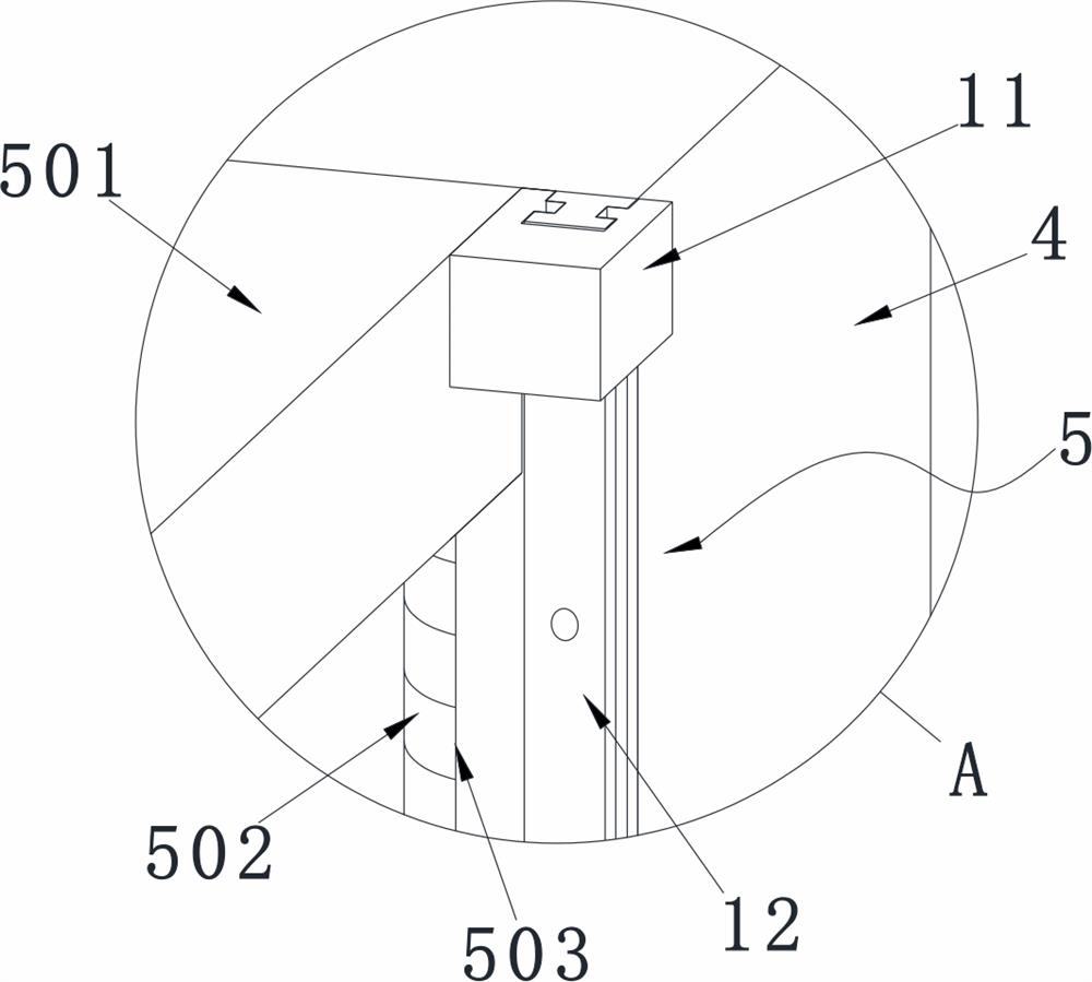
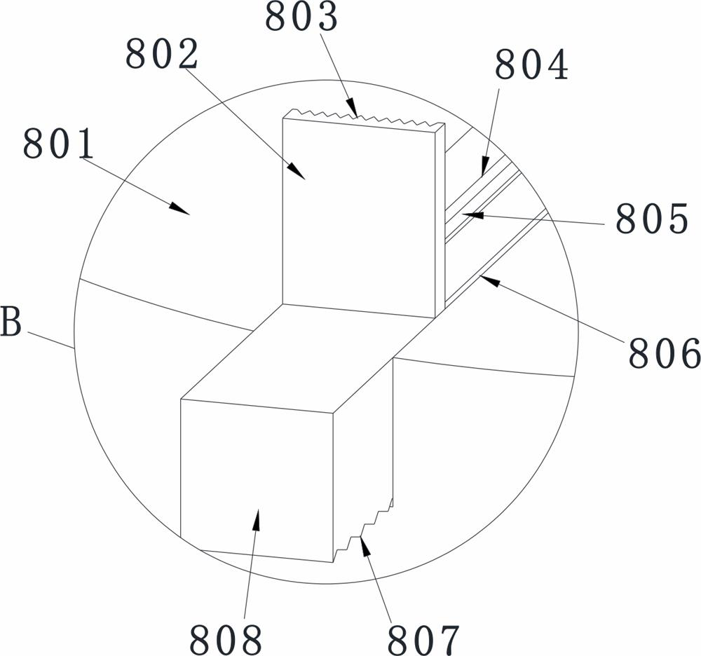
[0041] see Figure 1-11 , the present invention provides a technical solution: a PCB board drilling defect detection device, including a working box 1, a counterweight 14 is installed in the center of the inner bottom surface of the working box 1, and one side of the inner bottom surface of the working box 1 is fixedly connected There is a circuit board 13, and an image processing module 15, a matching module 16, a comparison module 17, a defect marking module...


PUM


Abstract

The invention discloses a PCB drilling defect detection device which comprises a working box body, a supporting column is installed at one corner of the top of the working box body, a display is fixedly connected to the top of the supporting column, a rapid clamping mechanism is installed in the center of the top of the working box body, a stand column is installed on one side of the top of the working box body, and a lifting mechanism is installed in the stand column. Through the arrangement of the lifting mechanism, the lifting of an image acquisition module is realized, the height of the image acquisition module can be adjusted according to the actual condition of a shot PCB, through the arrangement of the rapid clamping mechanism, a servo motor is utilized to drive a clamping head to perform centering clamping, the quick positioning and clamping of the PCB are realized, and manual operation is not needed. The device greatly reduces the labor cost, removes the redundancy and interference noise of the collected image through the image processing module, greatly improves the definition of the image, and marks the found defects through the defect marking module, thereby facilitating the checking of a worker.

Description

technical field [0001] The invention relates to the technical field of defect detection equipment, in particular to a PCB board drilling defect detection device and detection method. Background technique [0002] The Chinese name of PCB is printed circuit board, also known as printed circuit board, which is an important electronic component, a support for electronic components, and a carrier for electrical interconnection of electronic components. Known as a "printed" circuit board, the PCB board will have certain defects due to equipment errors during the production process, so a device is needed to detect the defects of the PCB board; [0003] There are many types of PCB defect detection equipment on the market today, which can basically meet people's needs, but there are still some deficiencies. The specific problems are as follows: [0004] (1) The existing PCB defect detection equipment requires personnel to manually position and clamp the board during the detection pr...

Claims


Application Information

Patent Timeline
Patent Type & Authority Applications(China)
IPC IPC(8): G01N21/88G01N21/01B25H1/08B25H1/12B25B11/00
CPCG01N21/8851G01N21/01B25H1/08B25H1/12B25B11/00G01N2021/8887
Inventor 梁得强李国通李海拥
Owner 深圳市浩创盛科技股份有限公司
Why Eureka
Try Eureka