Semiconductor package including interposer

A packaging and semiconductor technology, applied in the direction of semiconductor devices, semiconductor/solid-state device components, electric solid-state devices, etc., can solve problems such as loss of electrical characteristics

Pending Publication Date: 2022-01-28
SAMSUNG ELECTRONICS CO LTD
View PDF1 Cites 0 Cited by
  • Summary
  • Abstract
  • Description
  • Claims
  • Application Information

AI Technical Summary

Problems solved by technology

However, as the number of stacked semiconductor chips increases, a shift occurs due to a difference in physical distance between a memory chip disposed on the uppermost layer and a memory chip disposed on the lowermost layer ( s k ew ), resulting in a loss of electrical characteristics as the uppermost memory chip is farther away from the buffer chip than the lowermost memory chip

Method used


Image

  • Semiconductor package including interposer
  • Semiconductor package including interposer
  • Semiconductor package including interposer

Examples


Embodiment Construction

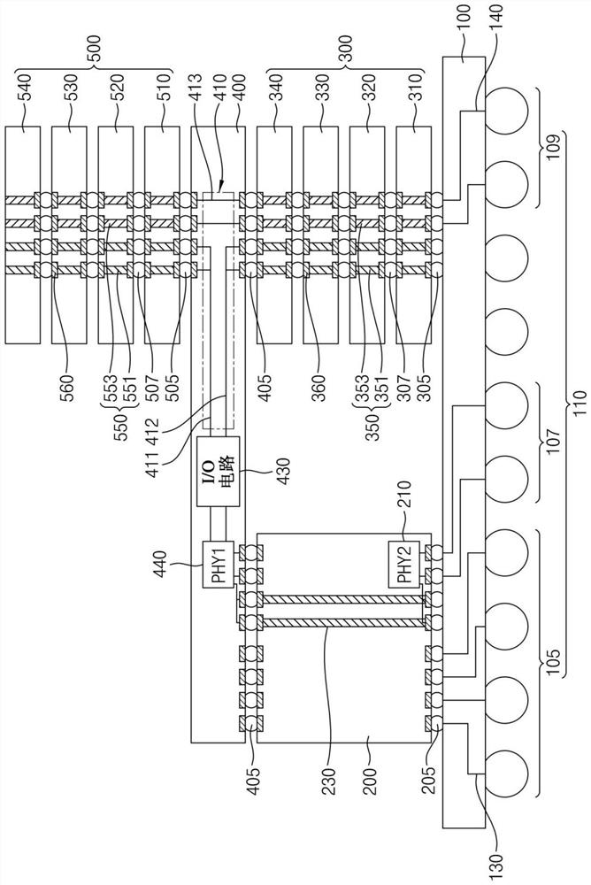
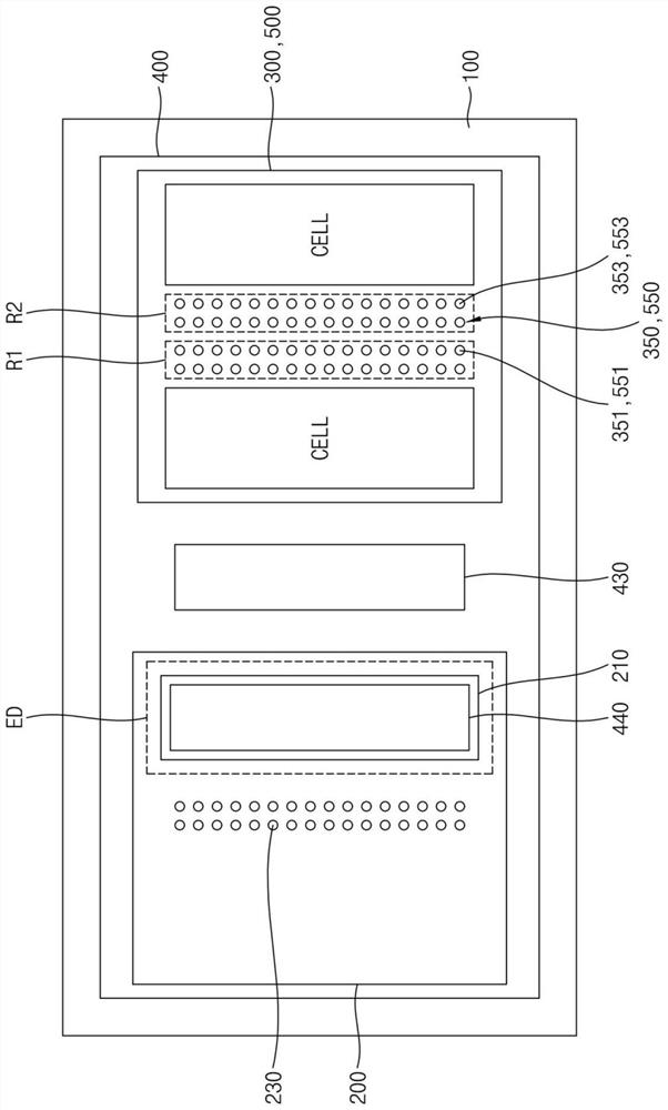
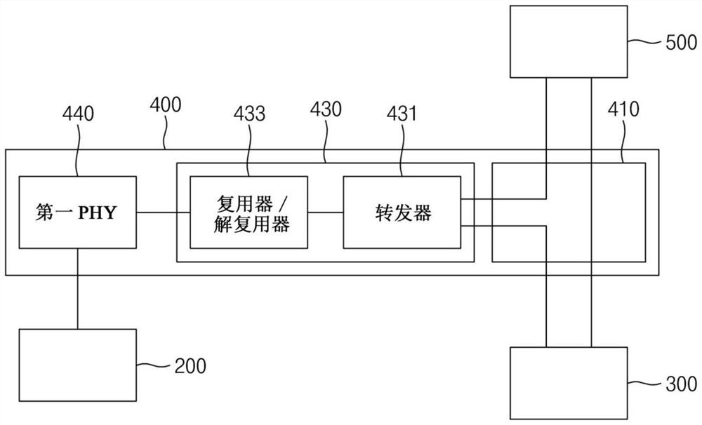
[0044] Figure 1A is a cross-sectional view illustrating a semiconductor package according to an embodiment of the present disclosure. Figure 1B is showing Figure 1A A schematic plan view of the semiconductor package shown. Figure 1C is a block diagram schematically illustrating an interposer according to an embodiment of the present disclosure.

[0045] refer to Figure 1A and Figure 1B, the semiconductor package may include a processor 200 , a lower memory 300 , an interposer 400 , and an upper memory 500 each disposed over a substrate 100 .

[0046] The substrate 100 may be a printed circuit board (PCB). The connection terminal 110 may be disposed under the substrate 100 . The connection terminal 110 may be a solder bump or a solder ball. The connection terminal 110 may include a data terminal 107 receiving a data signal from an external source and a plurality of power terminals 105 and 109 receiving a power signal. A plurality of wiring layers 130 and 140 electric...


PUM


Abstract

A semiconductor package includes a processor; a bottom memory containing a plurality of bottom memory chips stacked vertically; an interposer mounted on the processor and a lower memory; and an upper memory mounted on the interposer, the upper memory comprising a plurality of upper memory chips that are stacked vertically. The interposer includes a first physical layer (PHY) that sends and receives a signal between the processor and the lower memory and sends and receives a signal between the processor and the upper memory. The processor includes a second PHY communicating with the first PHY and a first through silicon via (TSV) electrically connecting the first PHY to the second PHY.

Description

[0001] Cross References to Related Applications [0002] This application claims priority from Korean Patent Application No. 10-2020-0093027 filed with the Korean Intellectual Property Office on July 27, 2020, the disclosure of which is incorporated herein by reference in its entirety. technical field [0003] The inventive concept relates to a semiconductor package, and more particularly, to a semiconductor package including an interposer. Background technique [0004] As the electronics industry progresses, electronic devices are gradually miniaturized and adapted to perform multiple tasks, and thus, the speed and capacity of memories applied to electronic devices are increasing. [0005] System-in-Package (SiP) technology has been developed to increase performance and reduce cost of electronic devices. According to this technology, a semiconductor memory device is integrated into one package structure together with a processing unit, so one semiconductor package product ...

Claims


Application Information

Patent Timeline
Patent Type & Authority Applications(China)
IPC IPC(8): H01L23/31H01L23/498H01L23/48H01L23/528
CPCH01L23/3128H01L23/49816H01L23/481H01L23/5283H01L23/5382H01L23/5385H01L25/18H01L2225/06541H01L2225/06513H01L2225/06517H01L2225/06572H01L2225/06527G11C5/025H01L24/05H01L24/13H01L24/16H01L24/17H01L24/48H01L24/73H01L24/81H01L25/0652H01L25/0657H01L2224/0557H01L2224/13101H01L2224/16145H01L2224/16146H01L2224/16225H01L2224/16235H01L2224/17181H01L2224/48091H01L2224/73207H01L2224/73257H01L2224/81801H01L2924/1432H01L2924/1434H01L2924/15174H01L2924/15192H01L2924/15311H01L2924/014H01L2924/00014H01L23/525H01L23/528H01L23/49827H01L24/97H01L23/49822H01L23/5383H01L2224/16147H01L2224/16165
Inventor 白起源
Owner SAMSUNG ELECTRONICS CO LTD
Why Eureka
Try Eureka