

Chip moving method and device
A chip and transfer chip technology, applied in the directions of transportation and packaging, conveyor objects, electrical components, etc., can solve the problem of low crystal bonding accuracy, and achieve the effect of improving accuracy
- Summary
- Abstract
- Description
- Claims
- Application Information
AI Technical Summary
Problems solved by technology
Method used
Image

Examples
Embodiment Construction
[0033] In order to make the purposes, technical solutions and advantages of the embodiments of the present application clearer, the technical solutions in the embodiments of the present application will be clearly and completely described below in conjunction with the drawings in the embodiments of the present application. Obviously, the described embodiments It is a part of the embodiments of this application, but not all of them. Based on the embodiments in the present application, all other embodiments obtained by persons of ordinary skill in the art without making creative efforts belong to the protection scope of the present application.
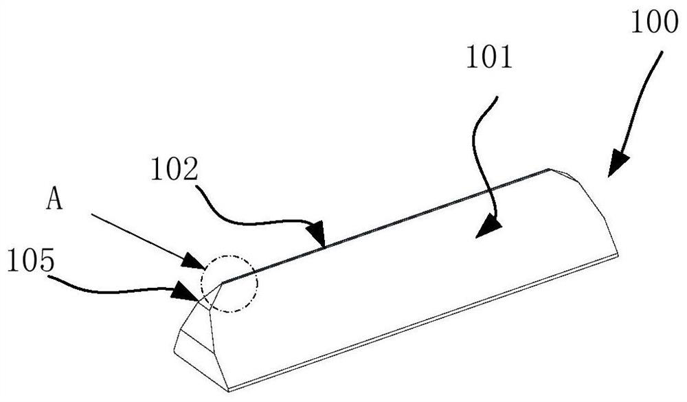
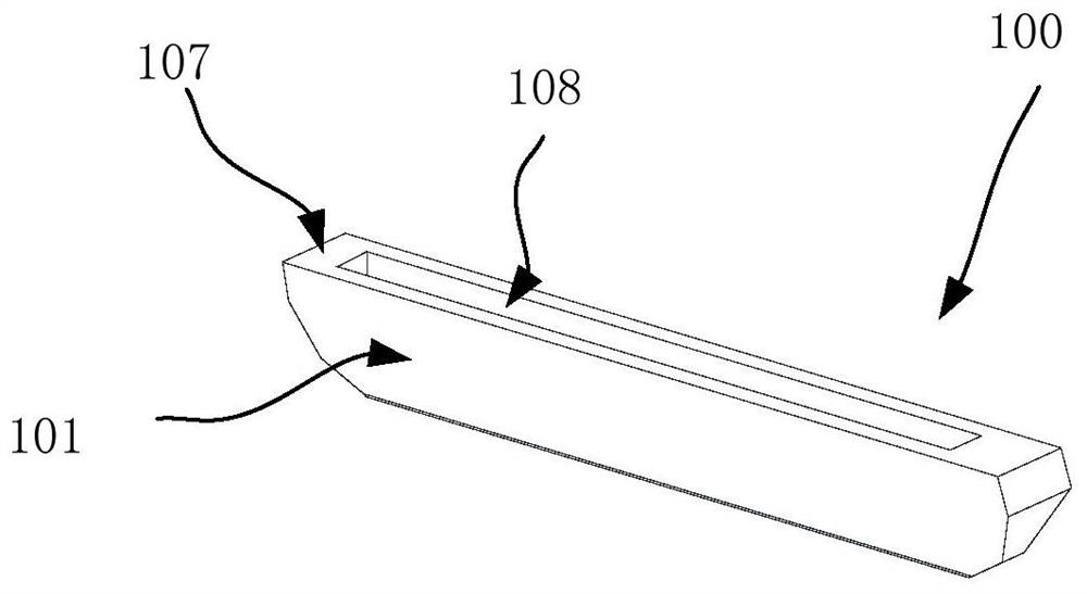
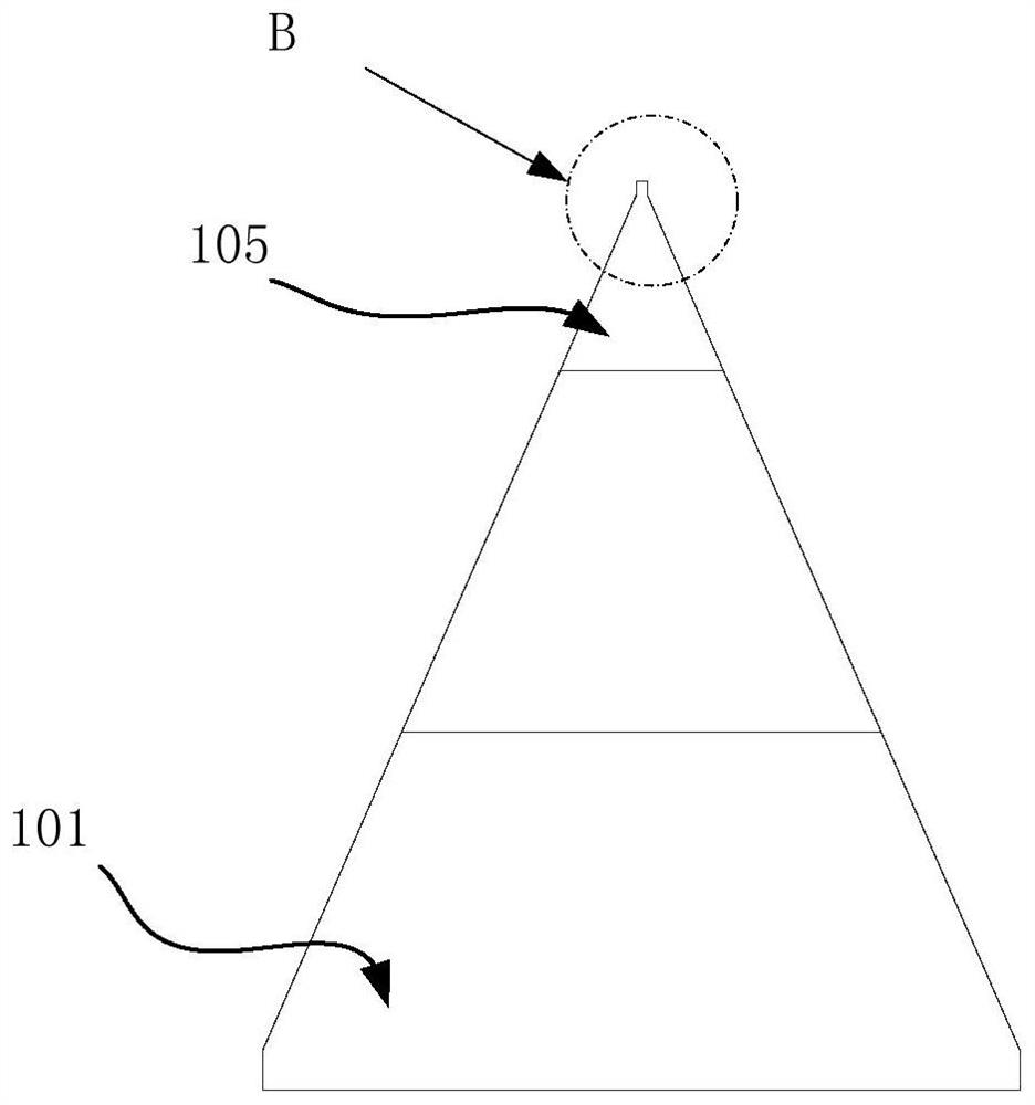
[0034] figure 1 A schematic structural diagram of the gas operation head provided in the embodiment of the present application; figure 2 Another schematic diagram of the structure of the gas operation head provided in the embodiment of the present application; image 3 yes figure 1 side view of Figure 4-Figure 7 yes figure 1 Vari...
PUM
 Abstract
Description
Claims
Application Information