Semiconductor sensor reverse packaging process

A packaging process and sensor technology, which is applied in semiconductor/solid-state device manufacturing, electromagnetic device manufacturing/processing, electrical components, etc., can solve the problem of inconvenient embedding of components into ceramic substrate pits, etc.

Pending Publication Date: 2022-02-08
福建福顺半导体制造有限公司
View PDF0 Cites 2 Cited by
  • Summary
  • Abstract
  • Description
  • Claims
  • Application Information

AI Technical Summary

Problems solved by technology

[0005] The invention provides a semiconductor sensor reverse packaging process, which solves the problem that the traditional semiconductor chip is inconvenient to be embedded in the ceramic substrate pit in the direction of the top of the base island and the pin

Method used


Image

  • Semiconductor sensor reverse packaging process
  • Semiconductor sensor reverse packaging process
  • Semiconductor sensor reverse packaging process

Examples


Embodiment Construction

[0030] The present invention will be further described below in conjunction with the accompanying drawings and embodiments.

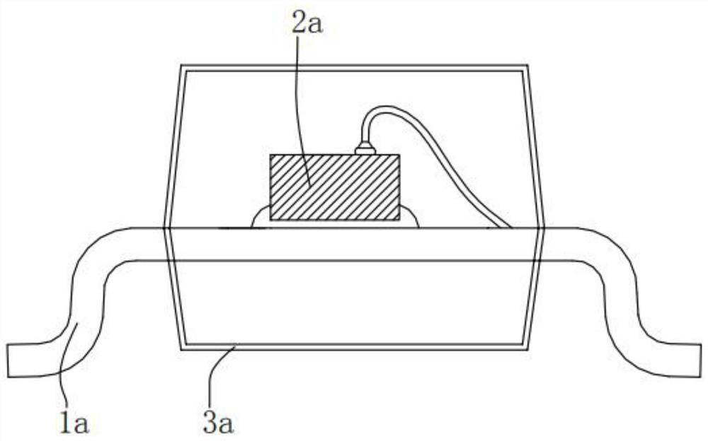
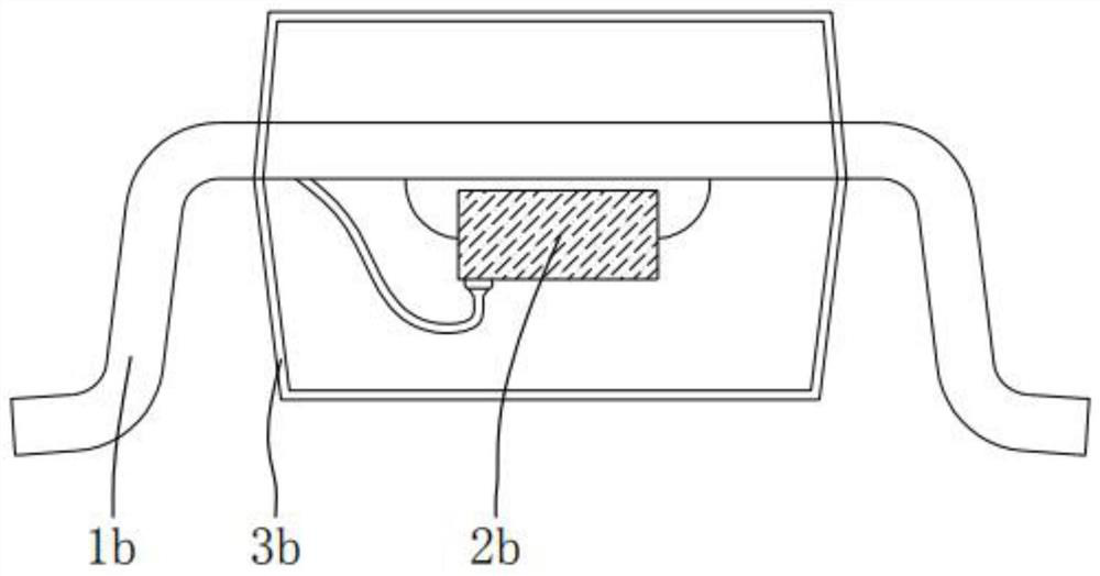
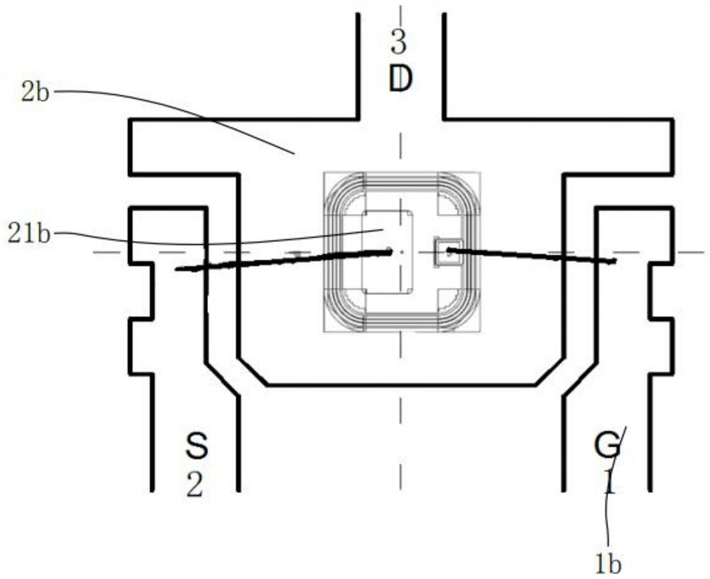
[0031] Please refer to figure 1 , figure 2 , image 3 , Figure 4 , Figure 5 , Figure 6 and Figure 7 ,in, figure 1 It is a structural schematic diagram of the prior art; figure 2 A schematic diagram of the back-sealing structure of the semiconductor sensor back-packing process provided by the present invention; image 3 for figure 2 The wiring diagram of the anti-base island part shown; Figure 4 The chip loading direction recognition diagram of the semiconductor sensor reverse packaging process provided by the present invention; Figure 5 A schematic structural view of the homogenizing equipment in the semiconductor sensor reverse packaging process provided by the present invention; Figure 6 for Figure 5 The enlarged schematic diagram of part A shown; Figure 7 for Figure 5 The enlarged schematic diagram of part B is shown.

[0...


PUM


Abstract

The invention provides a semiconductor sensor reverse packaging process. The semiconductor sensor reverse packaging process comprises a reverse packaging pin, a reverse packaging base island, a reverse packaging chip and a reverse packaging plastic sleeve. The semiconductor sensor reverse packaging process comprises the following steps: S1, preferentially aligning the reverse packaging chip to a connecting surface of the reverse packaging base island; s2, performing tin soldering connection on the circuit end of the reverse packaging chip and the circuit end of the reverse packaging base island; and S3, fixing the top of the reverse packaging base island in a reverse concave structure of the pin. The semiconductor sensor reverse packaging process provided by the invention has the advantages that reverse molding is carried out when components are subjected to plastic package molding, and the semiconductor sensor chip is structurally kept at the bottom position of the frame, so that after the semiconductor chip in a plastic package body enters a ceramic substrate, the sensor part is still in the front direction of the whole module, so that the function of the sensor is realized; and meanwhile, the reverse sealing process can realize the normal line signal connection between the sensor type component and other universal PCBs, and the sensor type component is not influenced by the interference of other external signals.

Description

technical field [0001] The invention relates to the technical field of semiconductor packaging, in particular to a semiconductor sensor reverse packaging process. Background technique [0002] The chip is an important part of the semiconductor device. During the processing of the semiconductor, the semiconductor chip and the carrier need to be welded to form a stable connection. The lead is the output terminal of the semiconductor chip information. After the semiconductor chip is welded, the two leads of the semiconductor need to be connected. Welding, after the welding is completed, the chip needs to be packaged. [0003] At present, SMD electronic components products use semiconductor chips on the base island and the top of the pins in the direction such as figure 1 As shown, the Hall sensor is different from the general SMT patch process on the front of the PCB. It is necessary to embed the element into the pit of the ceramic substrate, and the sensor semiconductor chip ...

Claims


Application Information

Patent Timeline
Patent Type & Authority Applications(China)
IPC IPC(8): H01L21/50H01L21/56H01L21/67H01L43/14
CPCH01L21/50H01L21/563H01L21/67121H10N52/01
Inventor 陈力
Owner 福建福顺半导体制造有限公司
Why Eureka
Try Eureka