
PM display panel and display device

A display panel and display area technology, applied in the direction of electrical components, electric solid devices, circuits, etc., can solve the problems of large heat generation, high energy consumption, uneven brightness, etc., to improve imaging quality, solve the limited number, overcome crosstalk effect

Pending Publication Date: 2022-02-08
义乌清越光电技术研究院有限公司
View PDF0 Cites 0 Cited by
  • Summary
  • Abstract
  • Description
  • Claims
  • Application Information

AI Technical Summary

Problems solved by technology

Due to the unique driving method of PMOLED, there are problems of high energy consumption, high heat generation, and uneven brightness

Method used


Image

  • PM display panel and display device
  • PM display panel and display device
  • PM display panel and display device

Examples


Embodiment Construction

[0024] The present invention will be further described in detail below in conjunction with the accompanying drawings and embodiments. It should be understood that the specific embodiments described here are only used to explain the present invention, but not to limit the present invention. In addition, it should be noted that, for the convenience of description, only some structures related to the present invention are shown in the drawings but not all structures.

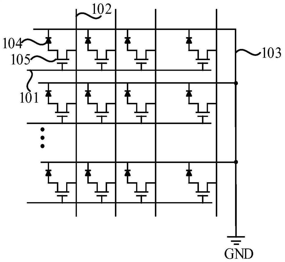
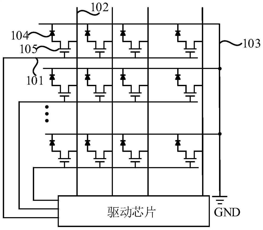
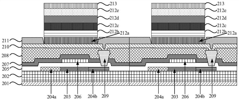
[0025] figure 1 It is a structural schematic diagram of a PM display panel provided by an embodiment of the present invention, refer to figure 1 , the embodiment of the present invention provides a PM display panel, which can be suitable for large-scale high-resolution panels, the PM display panel includes a display area and a non-display area, and the display panel also includes a plurality of first driving signal lines 101, a plurality of A second driving signal line 102, a plurality of thin film transistors 10...


PUM


Abstract

The embodiment of the invention discloses a PM display panel and a display device. The PM display panel comprises a display area and a non-display area, and further comprises a plurality of first driving signal lines, a plurality of second driving signal lines, a plurality of thin film transistors and a plurality of light emitting diodes. The plurality of thin film transistors and the plurality of light emitting diodes are located in the display area and are arranged in an array; grid electrodes of the thin film transistors in each row are connected with a first driving signal line; the first electrode of each column of thin film transistors is connected with a second driving signal line; the second pole of one thin film transistor is connected with the first pole of one light-emitting diode, and the first poles of the light-emitting diodes connected with the thin film transistors in the same row are mutually connected. According to the embodiment of the invention, the thin film transistor is introduced into the PM display panel, the grid electrode of the transistor can independently control the on or off of the light-emitting diode, crosstalk between pixel points is avoided, more light-emitting diodes can be arranged, the problem that the size and number of the pixel points are limited is solved, and the imaging quality of the PM display panel is effectively improved.

Description

technical field [0001] Embodiments of the present invention relate to display technologies, and in particular, to a PM display panel and a display device. Background technique [0002] PMOLED (Passive Matrix OLED, Passively Driven Organic Light-Emitting Diode), a cathode and an anode form a matrix, and light up the pixels in the array in a scanning manner. Each pixel operates in a short pulse mode and emits light with instantaneous high brightness. The advantage is that the structure is simple, which can effectively reduce the manufacturing cost. However, the high driving voltage and high current make PMOLED unsuitable for large-size and high-resolution panels, which is different from the current development. With the in-depth application of PMOLED in various fields, the market puts forward higher requirements for product size diversification, which requires the optimization and upgrading of PMOLED driving methods. Due to the unique driving method of PMOLED, there are probl...

Claims


Application Information

Patent Timeline
IPC IPC(8): H01L27/32
CPCH10K59/122H10K59/123H10K59/1315H10K59/1213
Inventor 周旭马中生穆欣炬唐鹏宇
Owner 义乌清越光电技术研究院有限公司
Learn More