4H-SiC metal semiconductor field effect transistor with P-type doped region and recessed buffer layer

A metal semiconductor and field effect transistor technology, applied in semiconductor devices, electrical components, circuits, etc., can solve the problems of reducing effective channel resistance, breakdown voltage drop, breakdown voltage deterioration, etc., to improve breakdown voltage, breakdown The effect of increasing the breakdown voltage and increasing the saturation current

Pending Publication Date: 2022-02-08
XIDIAN UNIV
View PDF13 Cites 0 Cited by
  • Summary
  • Abstract
  • Description
  • Claims
  • Application Information

AI Technical Summary

Problems solved by technology

Although compared with the traditional results, the saturation drain current and frequency of the double-recessed 4H-SiC MESFET have been greatly improved, but its breakdown voltage is much lower than that of the traditional structure.
This is an unavoidable problem that needs to be balanced in power devices: a wide channel brings a large saturated drain current, but at the same time it also reduces the effective resistance of the channel, resulting in a deterioration of the breakdown voltage

Method used


Image

  • 4H-SiC metal semiconductor field effect transistor with P-type doped region and recessed buffer layer

Examples


Embodiment 1

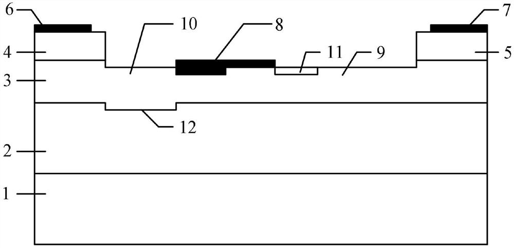
[0021] Such as figure 1 As shown, a 4H-SiC metal-semiconductor field-effect transistor with a P-type doped region and a recessed buffer layer includes, from bottom to top: 4H-SiC semi-insulating substrate 1, P-type buffer layer 2, and N-type channel layer 3 , the doping concentration of the P-type buffer layer 2 is 1.4×10 15 cm -3 , with a thickness of 0.5 μm; the doping concentration of the N-type channel layer 3 is 3×10 17 cm -3 , with a thickness of 0.25 μm; both sides of the N-type channel layer 3 are respectively 0.5 μm long N + type source cap layer 4 and drain cap layer 5, both of which have the same doping concentration and thickness and are respectively 1.0×10 20 cm -3 and 0.2 μm, the surface of the source cap layer 4 and the drain cap layer 5 is respectively the source electrode 6 and the drain electrode 7, and a recessed channel surface is formed between the source electrode 6 and the drain electrode 7, and the N-type channel layer 3 Above and 0.5 μm away from...

Embodiment 2

[0025] A 4H-SiC metal-semiconductor field-effect transistor with a P-type doped region and a recessed buffer layer, including a doping concentration of 1×10 17 cm -3 The length and thickness of the P-type doped region are 0.2 μm and 0.05 μm respectively, and the depth of the recessed buffer layer is 0.03 μm.

[0026] The remaining technical solutions of this embodiment are consistent with Embodiment 1.

Embodiment 3

[0028] A 4H-SiC metal-semiconductor field-effect transistor with a P-type doped region and a recessed buffer layer, including a doping concentration of 4×10 17 cm -3 The length and thickness of the P-type doped region are 0.5 μm and 0.05 μm respectively, and the depth of the recessed buffer layer is 0.08 μm.

[0029] The remaining technical solutions of this embodiment are consistent with Embodiment 1.

[0030] Through simulation experiments, under the same conditions, compared with the double-recessed 4H-SiC metal-semiconductor field-effect transistor in the prior art, the breakdown voltage of the present invention has been improved by 61.57%, and the saturated drain current has also been improved to a certain extent, thus The output power density of the device is greatly improved, and the output power density is increased by about 72.85%.


PUM

PropertyMeasurementUnit
lengthaaaaaaaaaa
depthaaaaaaaaaa
lengthaaaaaaaaaa

Abstract

The invention relates to the technical field of field effect transistors, and discloses a 4H-SiC metal semiconductor field effect transistor with a P-type doped region and a recessed buffer layer. The field effect transistor comprises a 4H-SiC semi-insulating substrate, a P-type buffer layer and an N-type channel layer from bottom to top, the surface of the N-type channel layer is provided with a source electrode cap layer and a drain electrode cap layer, a source electrode and a drain electrode are arranged on the surface of the source electrode cap layer and the surface of the drain electrode cap layer respectively, a gate electrode is formed on the side, close to the source electrode cap layer, of the upper surface of the N-type channel, a concave gate-drain drift region is formed between the gate electrode and the drain electrode cap layer, a gate-source drift region is formed between the gate electrode and the source electrode cap layer, the surface of the concavegate-drain drift region is provided with a P-type doped region close to a gate corner, and the P-type buffer layer below the gate-source drift region is recessed downwards to form a recessed buffer layer. The field effect transistor has the advantages that the breakdown voltage is greatly improved, and the drain output current is stable.

Description

technical field [0001] The invention relates to the technical field of field effect transistors, in particular to a 4H-SiC metal semiconductor field effect transistor with a P-type doped region and a recessed buffer layer. Background technique [0002] Silicon carbide (SiC), as a third-generation new semiconductor material, exhibits excellent characteristics in many aspects, for example, it has 2-4×10 6 The high breakdown electric field of V / cm, the wide forbidden band of 3.3eV, the high thermal conductivity of 3.5W / (cm K) and the 2.7×10 7 cm / s high electron saturation velocity and other excellent characteristics. Among the many isomorphs of SiC, 4H-SiC has high electron saturation velocity and high electron mobility (the electron mobility of 4H-SiC is about twice that of 6H-SiC), and the ionization energy of its donor impurities Relatively small and low anisotropy, its overall performance is the most superior. Therefore, in radio frequency microwave power devices, 4H-SiC...

Claims


Application Information

Patent Timeline
Patent Type & Authority Applications(China)
IPC IPC(8): H01L29/06H01L29/812
CPCH01L29/8128H01L29/0619
Inventor 贾护军张云帆朱顺威杨银堂
Owner XIDIAN UNIV
Why Eureka
Try Eureka