
Semiconductor element and preparation method thereof

A semiconductor and component technology, applied in the field of semiconductor components and their preparation, can solve problems such as excessive spikes, MOSFET overvoltage failure, etc., achieve the effect of reducing the total charge, reducing VDS spikes, and ensuring good performance

Pending Publication Date: 2022-05-13
HUNTECK SEMICON (SHANGHAI) LTD
View PDF7 Cites 0 Cited by
  • Summary
  • Abstract
  • Description
  • Claims
  • Application Information

AI Technical Summary

Problems solved by technology

[0003] However, in practical applications, such as resonant topology power supply or brushless motor applications, the reverse recovery of the MOSFET body diode will be experienced during each switching process. When the body diode reverses recovery, the drain-source voltage VDS tends to spike too much and thus Directly lead to MOSFET overvoltage failure

Method used


Image

  • Semiconductor element and preparation method thereof
  • Semiconductor element and preparation method thereof
  • Semiconductor element and preparation method thereof

Examples


Embodiment Construction

[0060] The present invention will be further described in detail below in conjunction with the accompanying drawings and embodiments. It should be understood that the specific embodiments described here are only used to explain the present invention, but not to limit the present invention. In addition, it should be noted that, for the convenience of description, only some structures related to the present invention are shown in the drawings but not all structures.

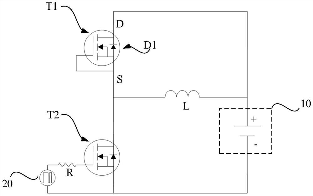
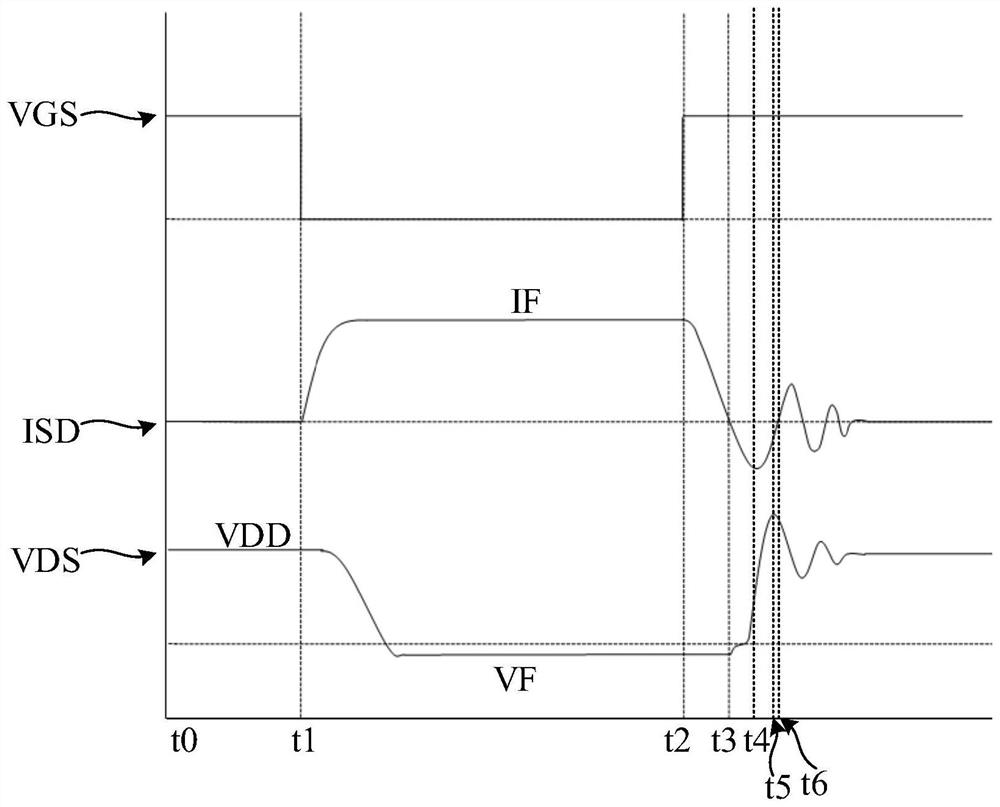
[0061] As mentioned in the background technology, the drain-source voltage VDS of the MOSFET tends to have too large spikes during the reverse recovery of the body diode. After research by the inventors, it is found that the details are: for example, refer to figure 1 , the first transistor T1 is an N-channel MOSFET under test, the second transistor T2 is an N-channel driving MOSFET, the power supply 10 is used to supply power to the first transistor T1, and the inductance L is used to simulate the stray inductance...


PUM


Abstract

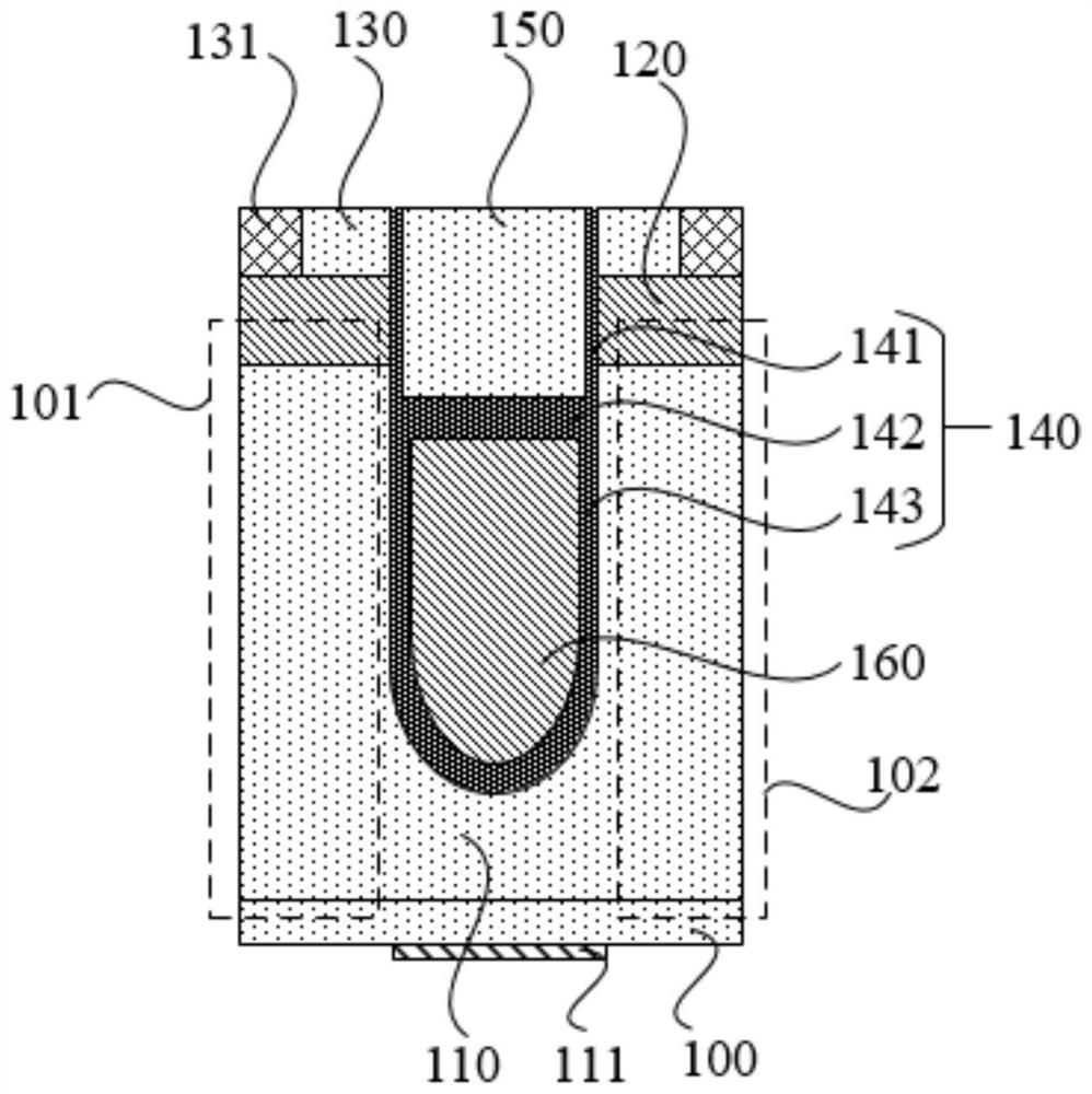
The embodiment of the invention discloses a semiconductor element and a preparation method thereof. In the semiconductor element, one side, far away from a substrate, of an epitaxial layer comprises a groove; the oxide layer is located in the groove; the grid polycrystalline silicon layer and the source polycrystalline silicon layer are embedded in the oxide layer, the grid polycrystalline silicon layer and the source polycrystalline silicon layer are separated by the oxide layer, and the oxide layer at least exposes the surface, away from the substrate, of the grid polycrystalline silicon layer; the body region and the source region are both formed in one end, far away from the substrate, of the epitaxial layer, the body region and the source region are both located on the left side and the right side of the grid polycrystalline silicon layer, and the body region is located on the side, close to the substrate, of the source region relative to the source region; the source electrode is located on the side, away from the substrate, of the body region and electrically connected with the source region; the source electrode polycrystalline silicon layer is electrically connected with the source electrode, and the type of doped ions of the source electrode polycrystalline silicon layer is opposite to that of doped ions of the grid electrode polycrystalline silicon layer; therefore, the total quantity of charges required by the MOSFET during reverse recovery of the body diode is reduced, and the peak of drain-source voltage VDS is reduced.

Description

technical field [0001] Embodiments of the present invention relate to the technical field of semiconductors, and in particular, to a semiconductor element and a manufacturing method thereof. Background technique [0002] Compared with the traditional Metal-Oxide-Semiconductor Field-Effect Transistor (MOSFET), the deep channel MOSFET has a better figure of merit (FOM). Due to the coupling balance design, the split gate power MOSFET can realize low on-resistance and low reverse transmission capacitance at the same time, thereby reducing the conduction loss and switching loss of the system and improving the efficiency of electronic products. [0003] However, in practical applications, such as resonant topology power supply or brushless motor applications, the reverse recovery of the MOSFET body diode will be experienced during each switching process. When the body diode reverses recovery, the drain-source voltage VDS tends to spike too much and thus Directly lead to MOSFET ov...

Claims


Application Information

Patent Timeline
Patent Type & Authority Applications(China)
IPC IPC(8): H01L29/78H01L29/49H01L29/45H01L21/336
CPCH01L29/7813H01L29/45H01L29/4916H01L29/66727H01L29/66734
Inventor 罗志云王飞潘梦瑜
Owner HUNTECK SEMICON (SHANGHAI) LTD
Learn More