Full-automatic double-head wafer testing machine

A wafer test, fully automatic technology, applied in the direction of chemical instruments and methods, cleaning methods and utensils, cleaning methods using tools, etc., to achieve the effect of improving accuracy and automation

Pending Publication Date: 2022-02-18
四川和恩泰半导体有限公司
View PDF9 Cites 0 Cited by
  • Summary
  • Abstract
  • Description
  • Claims
  • Application Information

AI Technical Summary

Problems solved by technology

[0004] In view of the above problems, the present invention provides a full-automatic double-head wafer testing machine, which solves the technical problem if the wafer is automatically detected

Method used


Image

  • Full-automatic double-head wafer testing machine
  • Full-automatic double-head wafer testing machine
  • Full-automatic double-head wafer testing machine

Examples


Embodiment Construction

[0028] The present invention will be further described below in conjunction with the accompanying drawings and embodiments.

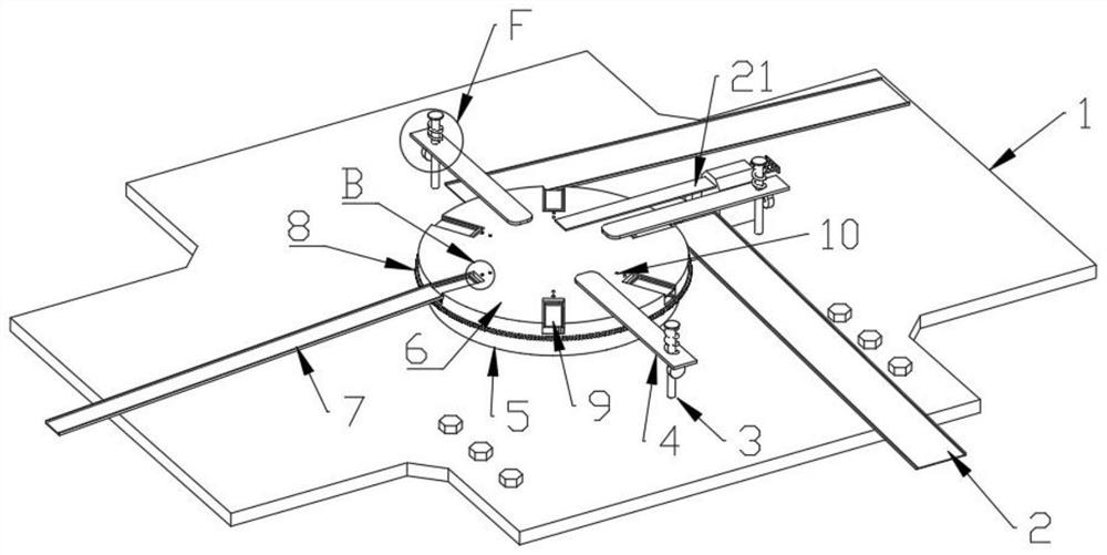
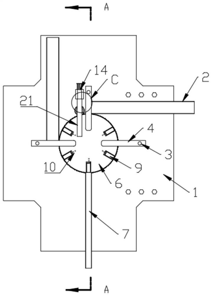
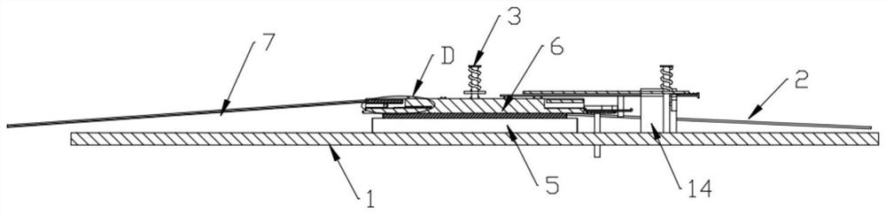
[0029] refer to Figure 1-10 , a fully automatic double-head wafer testing machine, including a test platform 1 and an electric turntable 5 installed on the upper end of the test platform 1. The rotating end of the electric turntable 5 is fixedly connected to a test disc 6. There are multiple equidistant distributions on the edge of the upper end of the test disc 6. The mounting groove 11 of the mounting groove 11 is slidably connected with a receiving plate 9 adapted to the wafer. The surface of the receiving plate 9 is provided with a groove, one side of which is open, and its size is adapted to the wafer, and the wafer can be positioned within it to limit For detection, different receiving plates 9 can be replaced according to the size of the wafer, so that different wafers can be detected.

[0030] The upper end of the test board 6 is fixedly conne...


PUM


Abstract

The invention provides a full-automatic double-head wafer testing machine. The full-automatic double-head wafer testing machine comprises a testing platform and an electric rotating disc installed at the upper end of the testing platform, wherein the rotating end of the electric rotating disc is fixedly connected with a testing disc, the edge of the upper end of the testing disc is provided with a plurality of mounting grooves distributed at equal intervals, the mounting grooves are internally provided with and slidably connected with bearing plates matched with wafers, the upper end of the testing disc is fixedly connected with a plurality of groups of conduction assemblies located on one sides of the mounting grooves, each conduction assembly comprises two metal contacts with a gap therebetween, the upper end of the testing platform is provided with an electric feeding sliding rail located on the first side of the testing disc, and three groups of testing devices are sequentially distributed at the upper end of the testing platform around the testing disc. According to the invention, technical problems in automatic detection of wafers are solved.

Description

technical field [0001] The invention relates to the technical field of wafer testing, in particular to a full-automatic double-head wafer testing machine. Background technique [0002] The chip is the light-emitting part of the LED lamp, and it is one of the most important parts inside. The chip is made of semiconductor materials, most of which are made of arsenic, aluminum, gallium and other materials. Changing its internal structure and material components can The wafers emit light of different colors. [0003] The surface of one end of the chip is smooth after being packaged, and the surface of the other end is soldered with two conductive metal bumps. The surface of the metal bumps will adhere to metal oxide layers or other stains during processing, which will affect its electrical conductivity. conduction test, but the existing wafer detection device cannot accurately and effectively detect and classify wafers in different conductive states, and the degree of automatio...

Claims


Application Information

Patent Timeline
Patent Type & Authority Applications(China)
IPC IPC(8): B07C5/344B07C5/02B07C5/36B08B1/02
CPCB07C5/344B07C5/02B07C5/362B08B1/02B08B1/008
Inventor 王悦聪徐艺凌
Owner 四川和恩泰半导体有限公司
Why Eureka
Try Eureka