SEMICONDUCTOR DEVICE and NONVOLATILE MEMORY DEVICE INCLUDING THE SAME

A semiconductor and device technology, applied in the field of semiconductor devices

Pending Publication Date: 2022-02-22
SAMSUNG ELECTRONICS CO LTD
View PDF0 Cites 0 Cited by
  • Summary
  • Abstract
  • Description
  • Claims
  • Application Information

AI Technical Summary

Problems solved by technology

Since the size of components (for example, transistors) included in a semiconductor device is also reduced as semiconductor devices become more highly integrated, there may be a problem that leakage current occurs

Method used


Image

  • SEMICONDUCTOR DEVICE and NONVOLATILE MEMORY DEVICE INCLUDING THE SAME
  • SEMICONDUCTOR DEVICE and NONVOLATILE MEMORY DEVICE INCLUDING THE SAME
  • SEMICONDUCTOR DEVICE and NONVOLATILE MEMORY DEVICE INCLUDING THE SAME

Examples


Embodiment Construction

[0031] In the following, reference will be made to Figure 1 to Figure 8 Semiconductor devices according to some embodiments are illustrated.

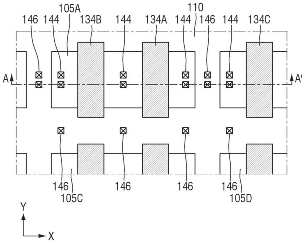
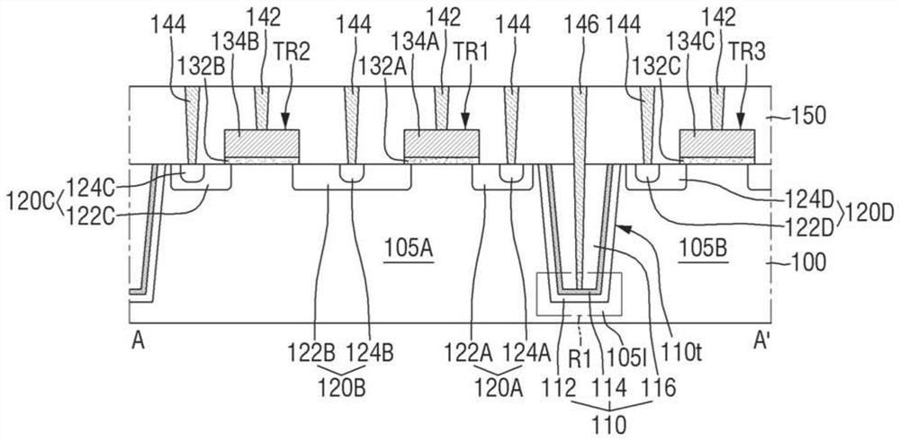
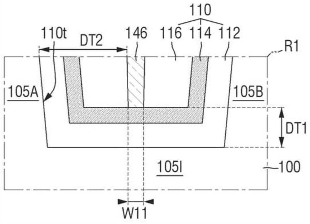
[0032] figure 1 is a layout diagram for illustrating a semiconductor device according to some embodiments. figure 2 is along figure 1 A schematic cross-sectional view taken along the line A-A'. Figure 3a and Figure 3b Yes figure 2 Various magnifications of the region R1.

[0033] refer to figure 1 , figure 2 and Figure 3a , the semiconductor device according to some embodiments may include a first substrate 100 , an element isolation film 110 , first to third circuit elements TR1 , TR2 and TR3 , an interlayer insulating film 150 , a gate contact 142 , a source / drain contact portion 144 and isolation contact portion 146 . For ease of explanation, figure 1 The gate contact 142 is not shown.

[0034] The first substrate 100 may include, but is not limited to, a base substrate and an epitaxial layer grown on the base subs...


PUM


Abstract

The invention provides a semiconductor device and a nonvolatile memory device. The semiconductor device includes: a substrate; an element isolation film defining a first active region in the substrate; a first gate electrode on the first active region; a first source / drain region inside the first active region between the element isolation film and the first gate electrode; and an isolation contact portion extending in a vertical direction intersecting an upper surface of the substrate in the element isolation film. The isolation contact is configured to be applied with a voltage.

Description

technical field [0001] The present disclosure relates to semiconductor devices. More specifically, the present disclosure relates to a semiconductor device including an element isolation film. Background technique [0002] With the development trend of electronic products to be light, thin, short and small, the demand for high integration of semiconductor devices is increasing. Since the size of components (eg, transistors) included in the semiconductor device is also reduced as the semiconductor device becomes more highly integrated, there may be a problem that leakage current occurs. Therefore, it may be advantageous to control the leakage current of semiconductor devices to improve the performance and reliability of the semiconductor devices. [0003] On the other hand, there is a need for semiconductor devices capable of storing large volumes of data in electronic systems using data storage. Therefore, methods for increasing the data storage capacity of semiconductor ...

Claims


Application Information

Patent Timeline
Patent Type & Authority Applications(China)
IPC IPC(8): H01L29/792H01L29/788H01L27/11524H01L27/11548H01L27/11556H01L27/1157H01L27/11575H01L27/11582
CPCH01L29/792H01L29/788H10B41/35H10B41/50H10B41/27H10B43/35H10B43/50H10B43/27H01L27/088H01L21/823481H01L21/765H01L21/76224H01L21/823475H10B43/40G11C5/06H01L29/0653
Inventor 金鹤善高秉柱白圣权徐载和李昌宪
Owner SAMSUNG ELECTRONICS CO LTD
Why Eureka
Try Eureka