Silicon wafer separating device

A technology for silicon wafers and conveying devices, which is applied in transportation and packaging, electrical components, semiconductor/solid-state device manufacturing, etc. It can solve the problems of difficult separation of bonded n-sides, easily damaged silicon wafers, and low slicing efficiency, achieving fast Fragmentation, reduce bad film rate, save labor effect

Pending Publication Date: 2022-02-25
ZHANGJIAGANG DECHANG AUTOMATIC CO LTD
View PDF0 Cites 0 Cited by
  • Summary
  • Abstract
  • Description
  • Claims
  • Application Information

AI Technical Summary

Problems solved by technology

[0002] In the semiconductor production process, the semiconductor silicon wafer is divided into n-side and p-side after sintering, and the n-side of adjacent silicon wafers will be bonded together. At present, manual segmentation is used. Due to the high bonding force of sintering, it is difficult to bond the n-side Separated, so it must be soaked in acid for a long time, and then manually divided into slices, even so, it is relatively easy to damage the silicon wafer, and the slice efficiency is low

Method used


Image

  • Silicon wafer separating device

Examples


Embodiment Construction

[0015] The technical solutions in the embodiments of the present invention will be described in detail below in conjunction with the accompanying drawings in the embodiments of the present invention. Obviously, the described embodiments are only some of the embodiments of the present invention, not all of them. Based on the embodiments of the present invention, all other embodiments obtained by persons of ordinary skill in the art without making creative efforts belong to the protection scope of the present invention.

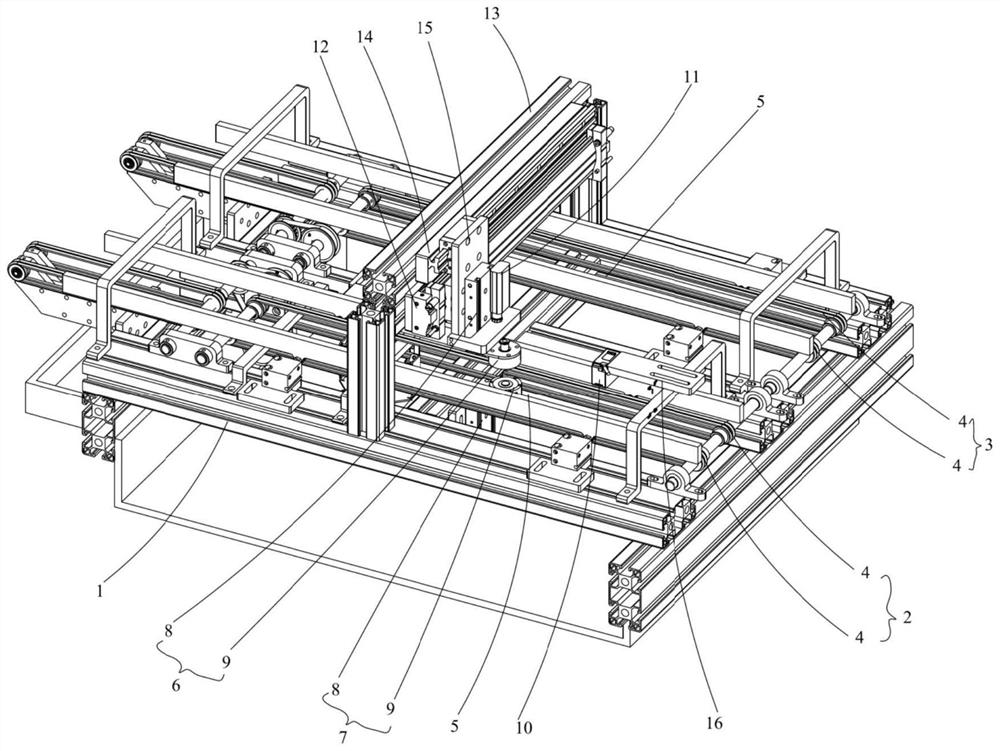
[0016] ginseng figure 1 As shown, the silicon chip slicing device in the present embodiment includes a frame 1, and the first conveying device 2 and the second conveying device 3 with the same structure are arranged side by side on the frame 1, and the first conveying device 2 includes side-by-side A pair of conveyor belts 4, a gap 5 is sandwiched between the pair of conveyor belts 4, a first suction cup device 6 and a second suction cup device 7 with the same ...


PUM


Abstract

The invention discloses a silicon wafer separating device. The device comprises a rack, a first conveying device and a second conveying device are arranged on the rack, the first conveying device comprises a pair of conveying belts, a first suction cup device and a second suction cup device are arranged above and below the first conveying device respectively, the first suction cup device comprises a lifting air cylinder and a suction cup, an image sensor and a thickness sensor are arranged above the first conveying device, and a translation air cylinder for driving the lifting air cylinder to move back and forth between the first conveying device and the second conveying device is arranged above the first conveying device. According to the silicon wafer separating device, an n surface and a p surface are distinguished through the image sensor, whether wafers are adhered or not is detected through the thickness sensor, the adhered wafers are separated through the suction cup devices arranged along a vertical direction, so that the silicon wafers with the p surface facing upwards and the silicon wafers with the n surface facing upwards are conveyed along the two conveying devices, wafer separation is fast, the automation level is high, wafer separation efficiency is improved, labor is saved, and the wafer rejection rate is reduced.

Description

technical field [0001] The present application relates to the field of silicon wafer slicing, in particular to a silicon wafer slicing device. Background technique [0002] In the semiconductor production process, the semiconductor silicon wafer is divided into n-side and p-side after sintering, and the n-side of adjacent silicon wafers will be bonded together. At present, manual segmentation is used. Due to the high bonding force of sintering, it is difficult to bond the n-side Separated, so it must be soaked in acid for a long time, and then manually sliced, even so, it is relatively easy to damage the silicon wafer, and the slice efficiency is low. Contents of the invention [0003] The object of the present invention is to provide a silicon chip slicing device to overcome the deficiencies in the prior art. [0004] To achieve the above object, the present invention provides the following technical solutions: [0005] The embodiment of the present application disclose...

Claims


Application Information

Patent Timeline
Patent Type & Authority Applications(China)
IPC IPC(8): H01L21/677H01L21/67H01L21/683
CPCH01L21/67706H01L21/6838H01L21/67276
Inventor 杨宣教
Owner ZHANGJIAGANG DECHANG AUTOMATIC CO LTD
Why Eureka
Try Eureka