
Silicon wafer separation and loading machine for silicon wafer production

A chip loading machine and silicon chip technology, which is applied in the direction of conveyor objects, transportation and packaging, and final product manufacturing, etc., can solve the problems of silicon chip damage, lack of monitoring, poor loading efficiency, etc., to ensure integrity and reduce Damage, benefit-increasing effects

Inactive Publication Date: 2019-07-26
江西宝群电子科技有限公司
View PDF0 Cites 0 Cited by
  • Summary
  • Abstract
  • Description
  • Claims
  • Application Information

AI Technical Summary

Problems solved by technology

At present, most enterprises that produce silicon wafers are manually loaded, and the silicon wafers are inserted into the wafer basket one by one. Due to the residual mortar between the silicon wafers and the force of water, the silicon wafers will be very adsorbed. However, due to the uneven force of manual loading, it is easy to break the silicon wafer, and the loading efficiency is also poor.
The shortcomings of the existing film loading device are mainly manifested in: 1. Insufficient in automation, manual operation is required, automatic production and automatic transmission operations are not possible, and a series of subsequent operations such as loading and unloading baskets are difficult to automate to the extent that it is inconvenient for the user to use the device
Second, the processing speed is insufficient
During the whole process of separation and transportation, the silicon wafer will be in contact with foreign objects, which can also damage the silicon wafer and increase the cost
There is also a lack of monitoring functions, and it is not yet able to connect with other devices

Method used


Image

  • Silicon wafer separation and loading machine for silicon wafer production
  • Silicon wafer separation and loading machine for silicon wafer production
  • Silicon wafer separation and loading machine for silicon wafer production

Examples


Embodiment 1

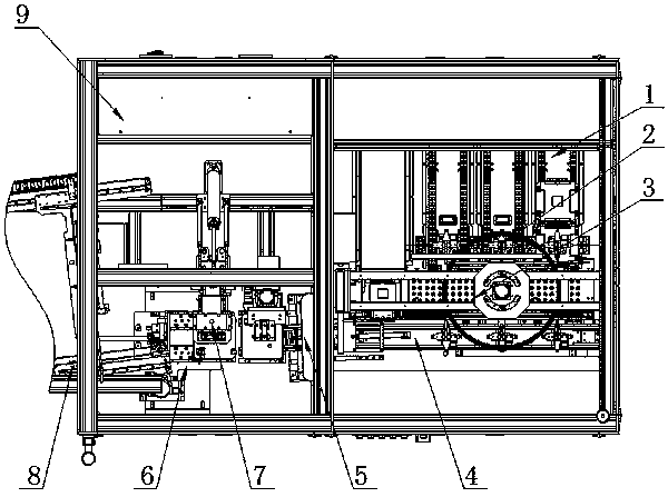
[0027]Embodiment 1, a kind of loading machine that is used for the production of silicon chip, comprises clip delivery module 1, splitting manipulator 2, splitting mechanism 3, conveying module 4, shaping module 5, insertion manipulator 6, empty Basket reflow module 7, flipping module 8, transplanting module 9, film loading machine frame 10; among them: clip conveying module 1, fragmentation manipulator 2, fragmentation mechanism 3, conveying module 4, shaping mold Group 5, inserting manipulator 6, empty basket return module 7, overturning module 8, and transplanting module 9 are all installed on the frame 10 of the chip loading machine, and a clip delivery module 1 and delivery module 4 are provided There is a fragmentation mechanism 3, a fragmentation manipulator 2 is installed on one side of the clip conveying module 1, a shaping module 5 is installed at the end of the conveying module 4, a turning module 7 is installed at the end of the shaping module 5, and the turning mod...

Embodiment 2

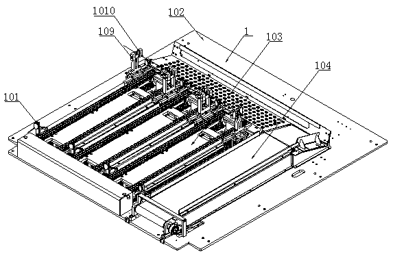
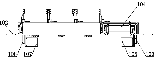
[0028] Embodiment 2, a chip loader for silicon wafer production, the clip conveying module 1 includes a first photoelectric sensor 101, a substrate assembly 102, a first conveying assembly 103, a first conveying assembly 104, and a first motor 105. The first high-torque synchronous toothed belt 106, the second motor 107, the second high-torque synchronous toothed belt 108, the air blowing plate 109, and the optical fiber 1010; wherein: the substrate assembly 102 is equipped with the second conveying assembly 104 and three A first conveying assembly 103, each first conveying assembly 103 both sides are equipped with air blowing board 109, each first conveying assembly 103 both sides are equipped with a first photoelectric sensor 101, substrate assembly 102 bottom is installed with a first Motor 105, second motor 107, the first motor 105 is connected with the first conveying assembly 104 through the first high torque synchronous belt 106, the second motor 107 is connected with th...

Embodiment 3

[0029] Embodiment 3, a kind of loading machine for the production of silicon wafers, the slicer mechanism 3 includes a bracket 301, a bearing seat 30, a rotating shaft 303, a turntable 304, a spacer 305, a first bearing 306, a second bearing 307, The third bearing 308, the fixed ring 309, the first coupling 3010, the third motor 3011, the first connecting plate 3012, the linear slider 3013, the mounting plate 3014, the vertical plate 3015, the adapter plate 3016, the suction cup 3017, the second Connecting plate 3018, third cylinder 3019; Wherein: bearing seat 302 is installed in the middle of support 301, bearing seat 302 is embedded with the bearing system that is formed by first bearing 306, second bearing 307, third bearing 308, fixed ring 309 , the rotating shaft 303 is installed on the lower part of the rotating disc 304, the rotating disc 304 is separated from the bearing seat 302 by the spacer 305, the fixed ring 309 is stuck in the slot of the rotating shaft 303, so th...


PUM


Abstract

The invention relates to a silicon wafer separation and loading machine for silicon wafer production. In a whole process of separation and conveying, a silicon wafer can be in contact with a foreign matter, so that the silicon wafer can be damaged, and the cost is increased. The machine has no monitoring function and cannot be connected with other equipment. The invention relates to the silicon wafer separation and loading machine for silicon wafer production, wherein the silicon wafer separation and loading machine comprises an elastic clamp conveying module, a separation mechanical arm, a separation mechanism, a conveying module, a shaping module, a silicon wafer inserting mechanical arm, an empty basket backflow module, a turnover module and a transplanting module which are all installed on a rack of the silicon wafer separation and loading machine, wherein the separation mechanism is arranged between the elastic clamp conveying module and the conveying module. According to the device, a silicon wafer separation and loading mechanism with a special structure is adopted to realize the process of separation and loading of the silicon wafers, and the silicon wafer separation and loading mechanism is highly automatic and is higher in speed, so that it is ensured that the silicon wafers can be separated quickly and accurately, the damage to the silicon wafers can be reduced, theintegrity of the silicon wafers can be guaranteed to the maximum degree, the benefits are increased, and the cost is lowered.

Description

technical field [0001] The invention relates to the technical field of silicon chip insertion machines, in particular to a chip loading machine used for silicon chip production. Background technique [0002] In the field of photovoltaics or semiconductors, the multi-wire cutting process is mostly used to turn silicon blocks into silicon wafers. Since this process uses steel wires to drive silicon carbide abrasives for cutting, there will be a lot of mortar attached to the silicon wafers after cutting. Washing can remove these mortars. Between cleaning, these silicon wafers need to undergo simple treatment, such as degumming, pre-cleaning to remove impurities such as strands and mortar on the surface of the silicon wafers, and finally insert the silicon wafers into the silicon wafer basket, and use acid and lye to clean the silicon wafers. Silicon wafers were cleaned ultrasonically. At present, most enterprises that produce silicon wafers are manually loaded, and the silico...

Claims


Application Information

Patent Timeline
Patent Type & Authority Applications(China)
IPC IPC(8): H01L21/67H01L21/677H01L31/18
CPCH01L21/67155H01L21/67703H01L31/1876Y02P70/50
Inventor 张志康何海涛孙文璐
Owner 江西宝群电子科技有限公司
Learn More