Charging circuit

A charging circuit and circuit technology, which is applied to battery circuit devices, circuit devices, collectors, etc., can solve the problems of inability to quickly and orderly switch between boost and step-down functions, single function, and high cost, and achieve a BUCK step-down circuit structure Optimized and unified, simple circuit structure, strong practical effect

Active Publication Date: 2022-03-18
SHENZHEN TECH UNIV
View PDF11 Cites 0 Cited by
  • Summary
  • Abstract
  • Description
  • Claims
  • Application Information

AI Technical Summary

Problems solved by technology

[0002] The boost circuit and the step-down circuit are two common charging circuits. In a charging circuit, the boost circuit and the step-down circuit are usually set independently. For example, a charging circuit with a boost circuit structure usually only has a boost function. A charging circuit with a step-down circuit structure usually only has a step-down function, and its function is usually relatively single. For occasions that require both a step-up function and a step-down function, a charging circuit usually cannot meet the requirements for use.
[0003] In order to overcome the defects of the above traditional charging circuit, the patent document of Chinese Patent No. ZL201921635496.4 discloses a voltage boosting circuit using a card reader. Voltage circuit, and then connect the two circuits to the power supply respectively, and output the boost power signal and the step-down power signal to the outside respectively; although the charging circuit structure has the functions of boosting and stepping down at the same time, it ensures the stability of the power supply voltage , to realize the stable switching of high and low voltages, but the structure of the charging circuit simply integrates the traditional boost circuit and step-down circuit into the same circuit, and the structure of the boost circuit and step-down circuit itself is not too big Changes, the boost circuit and the step-down circuit also work independently, and cannot quickly and orderly switch between the boost and step-down functions according to needs; and its structure is complex and the cost is relatively high

Method used


Image

  • Charging circuit
  • Charging circuit
  • Charging circuit

Examples


Embodiment Construction

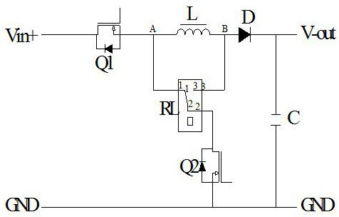
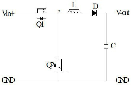
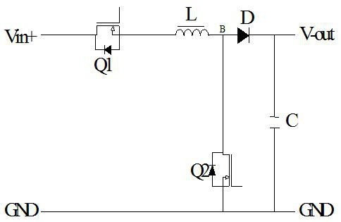
[0013] Referring to 1, the charging circuit of the present invention includes a charging circuit input terminal and a charging circuit output terminal, and a main circuit is formed between the circuit input terminal and the circuit output terminal, and the main circuit has a main circuit positive circuit and a main circuit grounding circuit . It should be noted that multiple components are connected to the positive circuit of the main circuit of the present invention, such as the main switching tube Q1, inductor L and diode D; the input end of the circuit can be connected to a power supply, and the output end of the circuit can be connected to a load.

[0014] As mentioned above, the components of the main circuit of the present invention include the main switching tube Q1, the inductor L and the diode D, and the main switching tube Q1, the inductor L and the diode D are sequentially connected in series along the extending direction from the input terminal to the output termina...


PUM


Abstract

A charging circuit comprises a charging circuit input end, a charging circuit output end and a main loop, a main switch tube, an inductor and a diode are sequentially connected in series on a positive pole line of the main loop, a positive pole end of the diode is connected with the inductor, and a negative pole end of the diode is connected with the output end of the charging circuit. A capacitor is electrically connected between the cathode end of the diode and the grounding wire of the main loop; and a control device is also arranged between the positive line of the main loop of the charging circuit and the grounding line of the main loop. The charging circuit provided by the invention has two functions of voltage boosting and voltage reducing at the same time, and can be switched between the voltage boosting function and the voltage reducing function as required.

Description

technical field [0001] The invention relates to a charging circuit. Background technique [0002] The boost circuit and the step-down circuit are two common charging circuits. In a charging circuit, the boost circuit and the step-down circuit are usually set independently. For example, a charging circuit with a boost circuit structure usually only has a boost function. A charging circuit with a step-down circuit structure usually only has a step-down function, and its function is usually relatively single. For a voltage stabilizing function that requires both a step-up function and a step-down function, a charging circuit usually cannot meet the use requirements. [0003] In order to overcome the defects of the above traditional charging circuit, the patent document of Chinese Patent No. ZL201921635496.4 discloses a voltage boosting circuit using a card reader. In this circuit, a voltage boosting circuit and a voltage reducing circuit are respectively provided. Voltage circ...

Claims


Application Information

Patent Timeline
Patent Type & Authority Applications(China)
IPC IPC(8): H02M3/04H02M3/158H02J7/00
CPCH02M3/04H02M3/1582H02J7/00H02J2207/20Y02T10/70
Inventor 王树晓
Owner SHENZHEN TECH UNIV
Why Eureka
Try Eureka