A grinding carrier, a grinding device, a grinding method, and a silicon wafer

A technology of grinding device and grinding method, which is applied in the fields of grinding method, silicon wafer, grinding device, and grinding carrier, which can solve the problems of grinding waste liquid overflow, downtime, and complicated installation, so as to save installation space and reduce secondary pollution Effect

Active Publication Date: 2022-06-07
XIAN ESWIN MATERIAL TECH CO LTD +1
View PDF9 Cites 0 Cited by
  • Summary
  • Abstract
  • Description
  • Claims
  • Application Information

AI Technical Summary

Problems solved by technology

However, in the existing grinding device for silicon wafers, a separate cleaning mechanism needs to be provided, so that the silicon wafer and the grinding stage are cleaned by the cleaning mechanism before and after the grinding of the silicon wafer is started, and then the water vapor two-fluid nozzle is used to clean the silicon wafer and the grinding stage. Rinse silicon wafers and grind the residual grinding liquid on the surface of the stage; the existing grinding device contains many mechanisms, the installation is complicated, and it is prone to failure and cause downtime, which affects the production efficiency of silicon wafers; at the same time, the existing grinding In the device, strip-shaped silicone strips or simple plate-shaped strip brushes are used to partition between two adjacent carrier plates. These two partition methods have poor sealing performance, and it is easy to cause the grinding waste liquid to overflow to the surface to be ground during the grinding process of silicon wafers. silicon wafers, resulting in secondary pollution of silicon wafers and carrier trays

Method used


Image

  • A grinding carrier, a grinding device, a grinding method, and a silicon wafer
  • A grinding carrier, a grinding device, a grinding method, and a silicon wafer
  • A grinding carrier, a grinding device, a grinding method, and a silicon wafer

Examples


Embodiment Construction

[0032] The technical solutions in the embodiments of the present invention will be clearly and completely described below with reference to the accompanying drawings in the embodiments of the present invention.

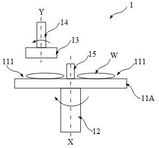
[0033] see figure 1 , which shows a schematic structural diagram of the existing grinding device 1 . like figure 1 As shown, the grinding device 1 mainly includes:

[0034] The grinding stage 11A is used to carry the silicon wafer W;

[0035] The first driving mechanism 12 is used to drive the grinding stage 11A to rotate around the first axis X during the grinding process;

[0036] The grinding head 13 is used for grinding the surface of the silicon wafer W;

[0037] The second driving mechanism 14 is used to drive the grinding head 13 to rotate around the second axis Y during the grinding process.

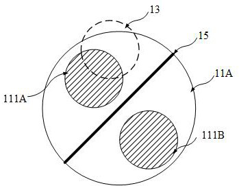
[0038] It should be noted that if figure 2 As shown, the grinding stage 11A is provided with a plurality of carrying trays 111 , and each carrying tray 111 can ca...


PUM

PropertyMeasurementUnit
angleaaaaaaaaaa

Abstract

The embodiment of the present invention discloses a grinding platform, a grinding device, a grinding method, and a silicon wafer; the grinding platform includes: a plurality of carrying disks for carrying silicon wafers; wherein, any two adjacent carrying disks A partition wall is arranged between them; a roller brush is arranged on one side of the partition wall, and the roller brush is used for scrubbing the grinding carrier and the silicon wafer; relative to the roller brush, it is arranged on the A liquid knife on the other side of the partition wall, the liquid knife is used to prevent the grinding waste liquid during the grinding process from overflowing to the surface of the silicon wafer to be ground.

Description

technical field [0001] Embodiments of the present invention relate to the technical field of semiconductor manufacturing, and in particular, to a grinding stage, a grinding device, a grinding method, and a silicon wafer. Background technique [0002] As a material for manufacturing semiconductor components, silicon wafer is a resource that is currently in short supply in the domestic market. Under normal circumstances, after the polysilicon is remelted and pulled, sliced, chamfered, ground, polished, cleaned, etc., chip-level silicon wafers with smooth and flat surfaces and neat edges can be obtained. Among them, the grinding process is an important process to remove the slicing marks of the silicon wafer, the surface damage layer and release the internal stress of the previous process. Therefore, the grinding process occupies an important position in the entire silicon wafer production process. [0003] The grinding process of the silicon wafer is mainly a process of redu...

Claims


Application Information

Patent Timeline
Patent Type & Authority Patents(China)
IPC IPC(8): B24B37/10B24B37/27B24B37/30B24B37/34H01L21/67H01L21/02
CPCB24B37/10B24B37/27B24B37/30B24B37/34H01L21/67092H01L21/02013
Inventor 刘玉乾
Owner XIAN ESWIN MATERIAL TECH CO LTD
Why Eureka
Try Eureka