Supercharge Your Innovation With Domain-Expert AI Agents!

Photoelectric detector chip, photoelectric detector chip circuit and photoelectric detector

A photoelectric detector and chip technology, applied in the field of optoelectronics, can solve the problems of insufficient photoelectric conversion efficiency of photodetector chips, and achieve the effects of improved photoelectric conversion efficiency, low coupling difficulty, and good device consistency

Pending Publication Date: 2022-03-25
THE 13TH RES INST OF CHINA ELECTRONICS TECH GRP CORP
View PDF5 Cites 0 Cited by
  • Summary
  • Abstract
  • Description
  • Claims
  • Application Information

AI Technical Summary

Problems solved by technology

[0004] In view of this, an embodiment of the present invention provides a photodetector chip, a photodetector chip circuit, and a

Method used


Image

  • Photoelectric detector chip, photoelectric detector chip circuit and photoelectric detector
  • Photoelectric detector chip, photoelectric detector chip circuit and photoelectric detector
  • Photoelectric detector chip, photoelectric detector chip circuit and photoelectric detector

Examples


Embodiment Construction

[0025] In the following description, specific details such as specific system structures and technologies are presented for the purpose of illustration rather than limitation, so as to thoroughly understand the embodiments of the present invention. It will be apparent, however, to one skilled in the art that the invention may be practiced in other embodiments without these specific details. In other instances, detailed descriptions of well-known systems, devices, circuits, and methods are omitted so as not to obscure the description of the present invention with unnecessary detail.

[0026] In order to illustrate the technical solutions of the present invention, specific examples are used below to illustrate.

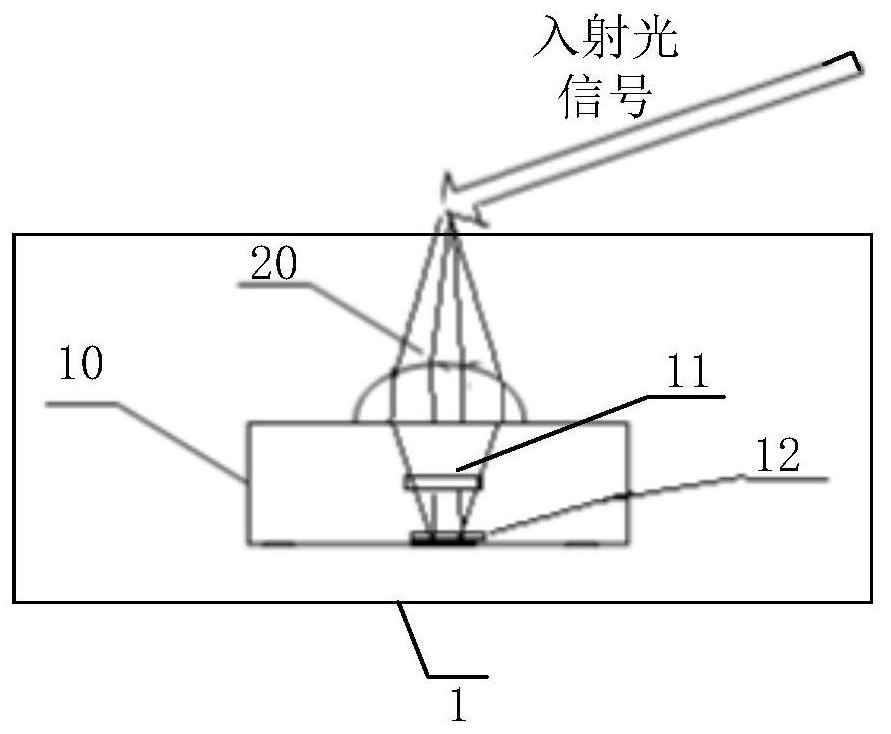
[0027] figure 1 The schematic structural diagram of the photodetector chip provided by the embodiment of the present invention is described in detail as follows.

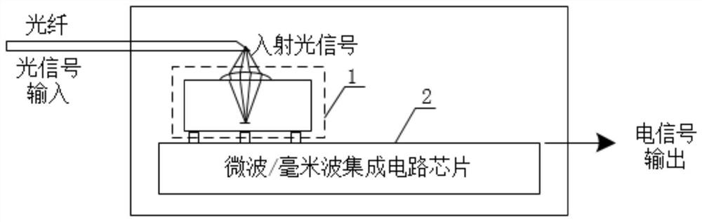
[0028] The photodetector chip 1 includes: a preset photodetector chip 10 and a converging lens 20 integr...


PUM


Abstract

The invention is applicable to the technical field of photoelectronics, and provides a photoelectric detector chip, a photoelectric detector chip circuit and a photoelectric detector, the photoelectric detector chip is composed of a preset photoelectric detector chip and a converging lens integrated on the preset photoelectric detector chip, the converging lens is used for converging the incident light signal to a photoelectric conversion photosensitive surface of a preset photoelectric detector chip. Because an incident light signal can be transmitted to the photoelectric conversion photosensitive surface of the preset photoelectric detector chip through a shorter optical path with smaller loss after being converged by the converging lens, more light with the same emergent power can be transmitted to the photoelectric conversion photosensitive surface of the photoelectric detector chip; therefore, the photoelectric conversion efficiency of the photoelectric detector chip is improved. And compared with the mode of coupling the optical lens and the preset photoelectric detector chip by adopting a saddle frame/angle iron and the like, the positioning precision is higher, the coupling difficulty is lower, and the consistency of the device is better.

Description

technical field [0001] The invention belongs to the technical field of optoelectronics, and in particular relates to a photodetector chip, a photodetector chip circuit and a photodetector. Background technique [0002] Microwave photonics is a fast-growing interdisciplinary subject, and it has been widely used in national defense, science and technology, and many aspects of daily life. Among them, the photodetector chip is the key component to realize photoelectric conversion, and is the core device in optical communication, microwave photonic radar and other systems. [0003] When the photodetector chip works, it needs to match the optical system of the signal, that is, the change center of the incident light needs to be within the linear range of the photoelectric characteristics of the photodetector. Because the incident light needs to be irradiated on the photoelectric conversion photosensitive surface of the device for photoelectric conversion, if the incident position...

Claims


Application Information

Patent Timeline
IPC IPC(8): H01L31/0232H01L25/16H03F3/195
CPCH01L31/02327H01L25/167H03F3/195
Inventor 许向前龚广宇卜爱民周彪李宇康晓晨邢星
Owner THE 13TH RES INST OF CHINA ELECTRONICS TECH GRP CORP
Features
  • R&D
  • Intellectual Property
  • Life Sciences
  • Materials
  • Tech Scout
  • Unparalleled Data Quality
  • Higher Quality Content
  • 60% Fewer Hallucinations
Learn More