
Optical detection device and method for three-dimensional structure of micro-nano device

An optical detection, three-dimensional structure technology, applied in the direction of using optical devices, measuring devices, instruments, etc., can solve the problems of measuring the internal structure of the device, affecting the measurement speed, and slow measurement speed.

Pending Publication Date: 2022-03-29
INST OF MICROELECTRONICS CHINESE ACAD OF SCI
View PDF0 Cites 0 Cited by
  • Summary
  • Abstract
  • Description
  • Claims
  • Application Information

AI Technical Summary

Problems solved by technology

[0005] (1) The measurement speed of the traditional method is slow, and it is impossible to measure the internal structure of the device without destroying the sample;
[0006] (2) Optical methods that can achieve non-destructive measurement usually require precise focusing, and repeated focusing is required when measuring the surface or internal structure of micro-nano devices at different heights, which affects the measurement speed;
[0007] (3) Optical methods usually can only reflect part of the structural information of the sample to be tested or the average parameter information of the array structure

Method used


Image

  • Optical detection device and method for three-dimensional structure of micro-nano device

Examples


Embodiment Construction

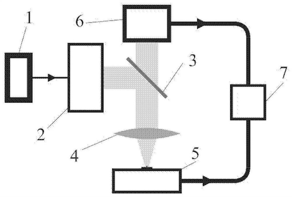
[0030] The invention irradiates the sample at the out-of-focus position with the converging light beam, and records the light intensity distribution of the reflected light field by the detector. The light beam sweeps across the sample to be tested horizontally at a certain step length. Since the sample is in a defocused position, the incident angles of different positions of the converging spot are different, and the impact of the sample to be tested on the reflected light field is also different. Therefore, the detector will record a series of slightly different reflected light field images, and select the data on the central axis of each image to form a new scanned composite image. At the same time, since the structural features and geometric parameters of the sample to be tested will affect the intensity distribution of the reflected light field, the structural features and geometric parameters of the sample to be tested can be obtained by comparing the measured scanned comp...


PUM


Abstract

A micro-nano device three-dimensional structure optical detection device comprises a light source, a light beam shaping module, a semi-transparent and semi-reflective mirror, a focusing lens, a translation stage, a detector and a computer, laser output by the light source is shaped and expanded through the light beam shaping module, parallel light beams after beam expansion are reflected by the semi-transparent and semi-reflective mirror and then focused by the focusing lens, and the parallel light beams are transmitted to the translation stage. Irradiating to a sample to be detected; placing a to-be-tested sample on the translation stage, wherein the to-be-tested sample is located at a defocus position; the reflected light beam sequentially passes through the focusing lens and the semi-transparent and semi-reflective mirror and then is detected by the detector; and the translation stage and the detector are controlled by the computer in a linkage manner, so that scanning and data acquisition are synchronously carried out. The device and the method provided by the invention can be used for measuring the line width, height / depth, side wall angle and parameter uniformity of lines and grooves, the diameter, height / depth, side wall angle and parameter uniformity of particles and holes, and can also be used for measuring complex structures such as S / L-shaped structures, array structures or multi-layer stacked structures.

Description

technical field [0001] The invention relates to the technical field of micro-nano scanning measurement, in particular to an optical detection device and method for a three-dimensional structure of a micro-nano device. Background technique [0002] The "ZTE incident" that occurred in 2018 made people realize that the independent development of the semiconductor industry plays a vital role in national economic development and industrial security. After decades of development, the performance of semiconductor devices has been greatly improved. With the improvement of performance, the feature size of the device structure is getting smaller and smaller, and the device structure is becoming more and more complex. In order to ensure device quality and yield, it is necessary to measure and analyze the three-dimensional feature size of semiconductor devices. [0003] The feature size of semiconductor devices is usually on the order of μm to nm. Traditional measurement methods incl...

Claims


Application Information

Patent Timeline
Patent Type & Authority Applications(China)
IPC IPC(8): G01B11/00G01B11/02G01B11/06G01B11/08G01B11/22G01B11/26G01B11/30B82Y35/00
CPCG01B11/00G01B11/02G01B11/0608G01B11/08G01B11/22G01B11/26G01B11/30B82Y35/00
Inventor 石俊凯李冠楠陈晓梅黎尧刘立拓高超董登峰周维虎
Owner INST OF MICROELECTRONICS CHINESE ACAD OF SCI
Features
  • Generate Ideas
  • Intellectual Property
  • Life Sciences
  • Materials
  • Tech Scout
  • Unparalleled Data Quality
  • Higher Quality Content
  • 60% Fewer Hallucinations
Learn More