A wafer surface cleaning device and method

A surface cleaning device and wafer technology, which is applied in the field of wafer processing, can solve the problems of high cost, low cleaning efficiency, and general cleaning effect, and achieve the effects of low cost, improved cleaning efficiency, and wide application range

Active Publication Date: 2022-05-17
ZHICHENG SEMICON EQUIP TECH (KUNSHAN) CO LTD
View PDF9 Cites 0 Cited by
  • Summary
  • Abstract
  • Description
  • Claims
  • Application Information

AI Technical Summary

Problems solved by technology

[0002] Wafer refers to the silicon wafer used to make silicon semiconductor circuits. It needs to be cleaned during the wafer processing process. The existing wafer cleaning device has complex structure, high cost, low cleaning efficiency and general cleaning effect, and still exists after cleaning. The problem of foreign matter sticking to the surface

Method used


Image

  • A wafer surface cleaning device and method
  • A wafer surface cleaning device and method
  • A wafer surface cleaning device and method

Examples


Embodiment 1

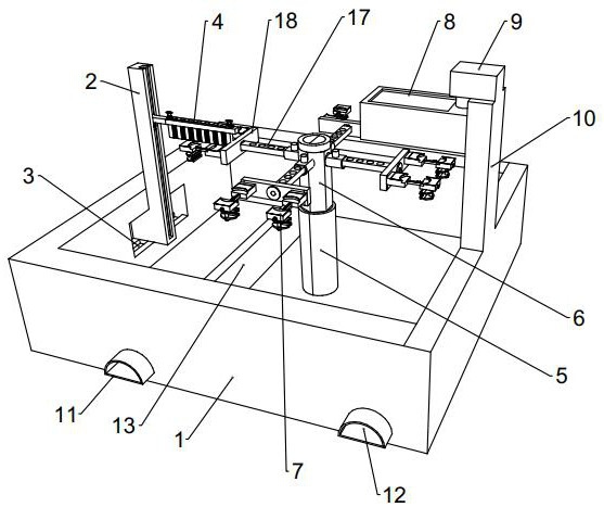
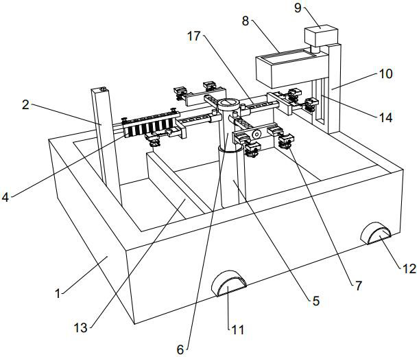
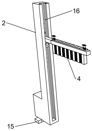
[0051] like figure 1 , 2 , 4 and 5, the present embodiment provides a wafer surface cleaning device, including a cleaning tank 1 and a cleaning mechanism, a cleaning mechanism and a wafer transport mechanism located in the cleaning tank 1; the cleaning mechanism includes a vertical rod 2, drive block 43 and cleaning brush 4, drive block 43 and vertical rod 2 are in vertical sliding connection, drive block 43 links to each other with cleaning brush 4 and can drive cleaning brush 4 to rotate; The cleaning assembly 8 connected by sliding in the direction, the cleaning assembly 8 is used for spraying and cleaning the wafer; It is arranged on the upper part of the vertical cylinder 5 and can rotate relative to the vertical cylinder 5. The rotary cylinder 6 is connected with a number of telescopic rods 17, and the end of the telescopic rod 17 is provided with a number of wafer clamping assemblies 7. The wafer clamping assemblies 7 are used for clamping Wafers of different sizes. ...

Embodiment 2

[0061] This embodiment provides a method for cleaning a wafer using the wafer surface cleaning device described in Embodiment 1, comprising the following steps:

[0062] (1) The push-pull vertical rod 2 moves to a suitable position in the horizontal direction, adjusts the height of the cleaning assembly by controlling the first cylinder 9, adjusts the height of the drum 6 and wafer clamping assembly 7 by controlling the second cylinder, and drives the Block 43 adjusts the height of the cleaning brush 4, and finally the cleaning brush 4 is located on the upper surface of the wafer holding assembly 7, so that the cleaning assembly is located above the wafer holding assembly 7;

[0063] (2) Adjust the position of the second clamping block 702 according to the size of the wafer to be cleaned, so that the wafer can be installed between the first clamping platform 703 and the second clamping platform 704;

[0064] (3) Place the wafer to be cleaned between the first clamping platform...

Embodiment 3

[0067] This embodiment provides a wafer surface cleaning device, including the structure in Embodiment 1.

[0068] like Figure 10 As shown, the bottom of the second clamping block 702 is connected with a screw 710, and the screw 710 is sleeved with two supporting platforms 711 arranged in parallel. The supporting platforms 711 are slidably connected with an adjustment plate 712, and the end of the adjustment plate 712 is connected with a support beam 713. , the first limit arc bar 714 and the second limit arc bar 715 are slidingly connected between the two support beams 713, and the angle between the planes where the first limit arc bar 714 and the second limit arc bar 715 are located is 15~30° °. After the fifth bolt 709 is unscrewed, the second clamping block 702 is moved along the slide bar 706 and disassembled, the second clamping block 702 is turned over so that one side of the supporting platform 711 faces upward, and then the second clamping block 702 is placed again ...


PUM


Abstract

The invention discloses a wafer surface cleaning device and method, comprising a cleaning tank, a cleaning mechanism, a cleaning mechanism and a wafer moving mechanism arranged in the cleaning tank; the cleaning mechanism includes a vertical rod, a driving block and a cleaning mechanism. brush, the driving block is slidably connected with the vertical rod in the vertical direction, the driving block is connected with the cleaning brush and can drive the cleaning brush to rotate; the cleaning mechanism includes a cleaning assembly that is slidably connected with the cleaning tank in the vertical direction, and The cleaning assembly is used to spray and clean the wafer; the wafer transport mechanism includes a vertical cylinder, a rotating cylinder, a telescopic rod and a wafer clamping assembly, and the rotating cylinder is arranged on the upper part of the vertical cylinder and can be opposed to each other. The rotating cylinder is connected with several telescopic rods, and the ends of the telescopic rods are provided with several wafer clamping components, and the wafer clamping components are used to clamp wafers of different sizes. The invention has wide application range, high cleaning efficiency and good cleaning effect on the wafer surface.

Description

technical field [0001] The invention belongs to the technical field of wafer processing, and in particular relates to a wafer surface cleaning device and method. Background technique [0002] Wafer refers to the silicon wafer used to make silicon semiconductor circuits. It needs to be cleaned during the wafer processing process. The existing wafer cleaning device has complex structure, high cost, low cleaning efficiency and general cleaning effect, and still exists after cleaning. The problem of foreign matter sticking to the surface. Contents of the invention [0003] The object of the present invention is to overcome the deficiencies in the prior art and provide a wafer surface cleaning device and method with wide application range, high wafer surface cleaning efficiency and good cleaning effect. [0004] The present invention provides following technical scheme: [0005] In the first aspect, a wafer surface cleaning device is provided, including a cleaning tank and a ...

Claims


Application Information

Patent Timeline
Patent Type & Authority Patents(China)
IPC IPC(8): B08B1/00B08B1/04B08B3/02B08B13/00
CPCY02P70/50
Inventor 万帮勇胡荪葳张祥
Owner ZHICHENG SEMICON EQUIP TECH (KUNSHAN) CO LTD
Why Eureka
Try Eureka