Oxide semiconductor film and semiconductor device

An oxide semiconductor and semiconductor technology, applied in semiconductor devices, semiconductor/solid-state device manufacturing, gaseous chemical plating, etc., can solve the problems of high insulation of alumina and difficulty in obtaining mixed crystals.

Pending Publication Date: 2022-04-12
FLOSFIA
View PDF4 Cites 1 Cited by
  • Summary
  • Abstract
  • Description
  • Claims
  • Application Information

AI Technical Summary

Problems solved by technology

However, alumina has high insulation and is difficult to dope, and its mobility is only 1-2 cm at most. 2 / Vs, it is difficult to obtain a mixed crystal of alumina and gallium oxide with excellent electrical properties

Method used


Image

  • Oxide semiconductor film and semiconductor device
  • Oxide semiconductor film and semiconductor device
  • Oxide semiconductor film and semiconductor device

Examples


Embodiment

[0072] 1. Membrane making device

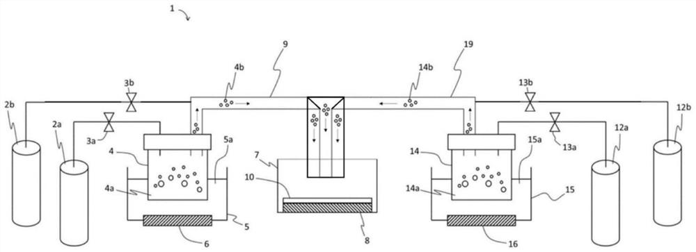
[0073] use figure 1 , illustrating the atomization CVD (Mist Chemical Vapor Deposition, atomization chemical vapor deposition) device (1) used in this embodiment. The atomizing CVD device (1) at least includes: a carrier gas source (2a, 12a) for supplying carrier gas, and a flow regulating valve (3a, 13a) for adjusting the flow rate of the carrier gas sent from the carrier gas source (2a, 12a) , an atomization source (4, 14) containing a raw material solution (4a, 14a), a container (5, 15) containing water (5a, 15a), an ultrasonic vibrator installed on the bottom surface of the container (5, 15) (6, 16), film forming chamber (7), supply pipes (9, 19) connecting the atomization generation source (4, 14) to the vicinity of the substrate (10), and a hot plate arranged in the film forming chamber (7) (8). Furthermore, a substrate (10) is arranged on the hot plate (8). In addition, there are two kinds of raw material solutions (4a, 14a), respe...

Embodiment 2

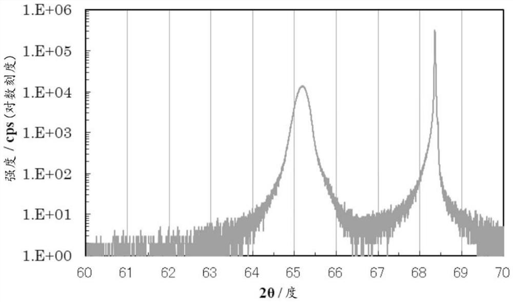
[0082] Film formation was performed in the same manner as in Example 1, except that the flow rate of the first carrier gas was 0.5 L / min and the film formation time was 3 hours. The film thickness of the obtained film was 1310 nm. As a result of film identification using an X-ray diffraction apparatus for the obtained film, the obtained film has a corundum structure (Al 0.15 Ga 0.85 ) 2 o 3 membrane. image 3 The measurement results of XRD are shown. For the obtained α-(Al 0.15 Ga 0.85 ) 2 o 3The electrical properties of the membrane are the same as in Example 1, the carrier type is n-type, and the carrier density and mobility are the same as in Example 1. The obtained film had a bandgap of 5.5 eV. In addition, the bandgap is calculated from the peaks of elastically scattered (zero energy loss) electrons and inelastically scattered (only partial loss of energy for interband transitions) electrons using reflection electron energy loss spectroscopy (REELS) . In addit...


PUM

PropertyMeasurementUnit
thicknessaaaaaaaaaa
band gapaaaaaaaaaa

Abstract

A first atomized droplet is generated by atomizing a first raw material solution containing at least aluminum, a second atomized droplet is generated by atomizing a second raw material solution containing at least gallium and a dopant, then the first atomized droplet is conveyed into a film-forming chamber using a first carrier gas, the second atomized droplet is conveyed into the film-forming chamber using a second carrier gas, and the second atomized droplet is conveyed into the film-forming chamber using a second carrier gas. The first atomized droplets and the second atomized droplets are mixed in a film forming chamber, and the mixed atomized droplets are thermally reacted near the surface of the substrate, thereby forming an oxide semiconductor film having a mobility of 5 cm2 / Vs or more and a metal oxide containing at least aluminum and gallium as the main component on the substrate.

Description

technical field [0001] The present invention relates to an oxide semiconductor film useful as a semiconductor, a semiconductor device and a semiconductor system using the oxide semiconductor film. Background technique [0002] Gallium oxide (Ga 2 o 3 ) semiconductor devices are attracting attention, and are expected to be applied to power semiconductor devices such as inverters. Furthermore, because of its wide bandgap, it is also expected to be used as light-emitting devices such as LEDs and sensors. According to Non-Patent Document 1, this gallium oxide can control the band gap by mixing crystals with indium and aluminum individually or in combination, and constitutes an attractive material system as an InAlGaO-based semiconductor. Here, the so-called InAlGaO-based semiconductor consists of In X Al Y Ga Z o 3 (0≤x≤2, 0≤y≤2, 0≤z≤2, X+Y+Z=1.5 to 2.5) means that all can be covered as the same material system including gallium oxide. [0003] Furthermore, in recent yea...

Claims


Application Information

Patent Timeline
Patent Type & Authority Applications(China)
IPC IPC(8): H01L29/24H01L29/872H01L29/739H01L29/778H01L29/78H01L29/808H01L29/812
CPCC23C16/40H01L21/20H01L29/24H01L29/78H01L29/872H01L29/7786H01L29/0619H01L29/0843H01L29/8083H01L29/045H01L33/42H01L29/7813H01L29/7395C23C16/403H01L29/12H01L29/7393H01L29/778H01L29/808H01L29/812H01L33/26
Inventor 菅野亮平
Owner FLOSFIA
Why Eureka
Try Eureka