MSM type deep ultraviolet photoelectric detector based on cubic boron nitride thick film and preparation method

A technology of boron nitride thick film and deep ultraviolet light, which is applied in the field of semiconductor photoelectric detection, can solve the problems of poor stability of thick film, weakened cubic phase performance, and poor crystal quality, so as to facilitate device integration and facilitate large-scale Effects of scale industrialization and enhanced adhesion

Active Publication Date: 2020-09-25
JILIN UNIV
View PDF9 Cites 1 Cited by
  • Summary
  • Abstract
  • Description
  • Claims
  • Application Information

AI Technical Summary

Problems solved by technology

[0005] The closest existing technology is to use cubic boron nitride single crystal synthesized by high temperature and high pressure to make deep ultraviolet photodetectors, but the size of single crystal synthesized by high temperature and high pressure is limited. At present, the largest one in the world is only 3 mm, which seriously hinders the future. device application
However, the growth of membrane materials is limited by internal stress. When the thickness gradually increases, the internal stress will continue to accumulate, which will cause the separation of the membrane base, so the stability of thick membranes is generally not good.
In addition, most cubic boron nitride films are mixed with a large number of hexagonal boron nitride phases, and this sp 2 The presence of the phase impairs the properties of the cubic phase
Obviously, the small crystal size and poor crystal quality of cubic boron nitride limit its application in deep ultraviolet photodetection

Method used


Image

  • MSM type deep ultraviolet photoelectric detector based on cubic boron nitride thick film and preparation method
  • MSM type deep ultraviolet photoelectric detector based on cubic boron nitride thick film and preparation method
  • MSM type deep ultraviolet photoelectric detector based on cubic boron nitride thick film and preparation method

Examples


Embodiment

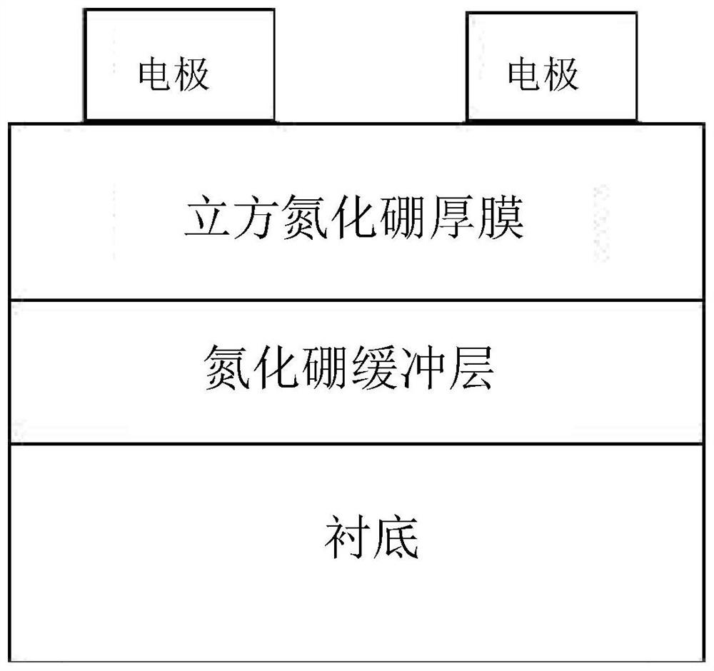
[0037] Preferably, the substrate is an n-type (100) silicon substrate with a thickness of 300 nm. The cut silicon wafers were ultrasonically cleaned in acetone, ethanol, and deionized water, then soaked in HF solution to remove surface oxides, dried with nitrogen and placed on the sample holder. The sample holder is sent into the magnetron sputtering chamber, and then vacuumized, when the vacuum reaches 10 -5 pa, heat the substrate to 600°C and continue to evacuate the chamber until it reaches 10 -5 Pa, the working gas nitrogen and argon are introduced into each 50sccm, and the working pressure is 2pa; the distance between the substrate and the target is 8cm; the negative bias voltage is 100V; the power of the radio frequency source is 120W; after pre-sputtering for 3 minutes, deposition for half an hour to obtain nitriding The boron buffer layer is then deposited for 2.5 hours to obtain a thick film of cubic boron nitride. Finally, electrodes were prepared on the surface of...


PUM

PropertyMeasurementUnit
thicknessaaaaaaaaaa
thicknessaaaaaaaaaa

Abstract

The invention discloses an MSM type deep ultraviolet photoelectric detector based on a cubic boron nitride thick film and a preparation method. The MSM type deep ultraviolet photoelectric detector comprises a substrate, a boron nitride buffer layer which is positioned on the substrate, a cubic boron nitride thick film which is positioned on the boron nitride buffer layer, and a pair of electrodeswhich are respectively stacked on the cubic boron nitride thick film. The electronic characteristics of the cubic boron nitride ultra-wide forbidden band, the stability in an extreme environment and other remarkable material performance advantages are utilized, the cubic boron nitride ultra-wide forbidden band is used as a light absorption layer, the photoelectric response of the device in a deepultraviolet region can be directly obtained, the dark current is low, the sensitivity is high, and the response speed is high; the MSM type deep ultraviolet photoelectric detector can be applied to extreme environments with high temperature, high pressure, high energy radiation and corrosivity, and has very high practical value in the fields of aerospace and information communication; the detectorcan be directly manufactured on a silicon-based substrate and can be compatible with an existing silicon-based process, device integration is facilitated, the process is simple, and large-scale industrialization is facilitated.

Description

technical field [0001] The invention belongs to the technical field of semiconductor photodetection, and in particular relates to a MSM type deep ultraviolet photodetector based on a cubic boron nitride thick film and a preparation method thereof. Background technique [0002] Ultraviolet detection technology is a new type of detection technology after infrared and laser detection technology. It has been widely used in astronomy, military, industry, scientific research and other fields. [0003] With the development and progress of science and technology, ultraviolet photodetectors made of silicon and GaAs materials can no longer meet people's needs. Due to the excellent performance of the third-generation wide-bandgap semiconductor materials, people began to consider their application in ultraviolet photodetection. Wide bandgap semiconductor materials with potential applications include diamond, SiC, group III nitrides, etc. [0004] Cubic boron nitride is a very typical...

Claims


Application Information

Patent Timeline
Patent Type & Authority Applications(China)
IPC IPC(8): H01L31/108H01L31/0304H01L31/18
CPCH01L31/1085H01L31/03044H01L31/1852H01L31/1856Y02P70/50
Inventor 殷红刘彩云高伟
Owner JILIN UNIV
Why Eureka
Try Eureka