
Diamond-like carbon protective film and preparation method thereof

A protective film and diamond technology, which is applied in the manufacture of microstructure devices, metal material coating technology, gaseous chemical plating, etc., can solve problems such as system failure, large thickness, and increased system size and weight

Pending Publication Date: 2021-04-27
ARMY ENG UNIV OF PLA
View PDF3 Cites 0 Cited by
  • Summary
  • Abstract
  • Description
  • Claims
  • Application Information

AI Technical Summary

Problems solved by technology

However, the thickness of the functional materials involved in the above-mentioned publications is too large when used, generally reaching more than 100 μm or even millimeter level, which is equivalent to or even exceeds the size of micro-nano electronic devices, which significantly increases the size and weight of the system.
[0003] At the same time, during the use of micro-nano electronic devices, the wear problem has become increasingly prominent, and long-term accumulation of wear will cause serious problems such as system failure

Method used


Image

  • Diamond-like carbon protective film and preparation method thereof

Examples


Embodiment 1

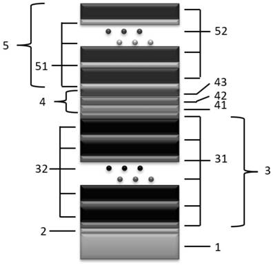
[0042] A diamond-like protective film, which sequentially includes a micro-nano electronic device substrate, a metal layer I, an insulating layer belt, an internal stress buffer layer and a wear-resistant layer belt from bottom to top; the insulating layer belt includes a silicon-containing thin layer and a non-doped Doped DLC layer, the bottom layer of the insulating layer is a silicon-containing thin layer, and then the non-doped DLC layer and silicon-containing thin layer are alternately distributed in turn, and the internal stress buffer layer includes H-W:DLC from bottom to top layer, M-W: DLC layer, L-W: DLC layer, the wear-resistant layer belt includes metal layer II and S-W: DLC layer, and the uppermost layer of the internal stress buffer layer is alternately distributed with metal layer II and S-W: DLC layer , the uppermost layer of the wear-resistant layer belt is a S-W:DLC layer.

[0043] The preparation method of above-mentioned diamond-like carbon protective film ...

Embodiment 2

[0056] A diamond-like protective film, which includes a micro-nano electronic device substrate, an insulating layer belt, an internal stress buffer layer and a wear-resistant layer belt from bottom to top; the insulating layer belt includes a silicon-containing thin layer and an undoped DLC layer, The bottom layer of the insulating layer belt is a silicon-containing thin layer, and then the non-doped DLC layer and the silicon-containing thin layer are alternately distributed in sequence, and the internal stress buffer layer includes H-W:DLC layer, M-W: DLC layer, L-W:DLC layer, the wear-resistant layer belt includes metal layer II and S-W:DLC layer, the uppermost layer of the internal stress buffer layer is alternately distributed with metal layer II and S-W:DLC layer, the wear-resistant The uppermost layer of the grinding belt is the S-W:DLC layer.

[0057] The preparation method of above-mentioned diamond-like carbon film comprises the steps:

[0058] S1: Select silicon mat...

Embodiment 3

[0067] A diamond-like protective film, which includes a micro-nano electronic device substrate, an insulating layer belt, an internal stress buffer layer and a wear-resistant layer belt from bottom to top; the insulating layer belt includes a silicon-containing thin layer and an undoped DLC layer, The bottom layer of the insulating layer belt is a silicon-containing thin layer, and then the non-doped DLC layer and the silicon-containing thin layer are alternately distributed in sequence, and the internal stress buffer layer includes H-W:DLC layer, M-W: DLC layer, L-W:DLC layer, the wear-resistant layer belt includes metal layer II and S-W:DLC layer, the uppermost layer of the internal stress buffer layer is alternately distributed with metal layer II and S-W:DLC layer, the wear-resistant The uppermost layer of the grinding belt is the S-W:DLC layer.

[0068] The preparation method of above-mentioned diamond-like carbon film comprises the steps:

[0069] S1: Select germanium m...


PUM

PropertyMeasurementUnit
Thicknessaaaaaaaaaa
Thicknessaaaaaaaaaa
Thicknessaaaaaaaaaa

Abstract

The invention discloses a diamond-like carbon protective film and a preparation method thereof. The diamond-like carbon protective film sequentially comprises a micro-nano electronic device base material, an insulating layer belt, an internal stress buffer layer and a wear-resistant layer belt from bottom to top, wherein the lowermost layer of the insulating layer belt is a silicon-containing thin layer, then undoped DLC layers and silicon-containing thin layers are sequentially and alternately distributed, the internal stress buffer layer sequentially comprises an H-W:DLC layer, an M-W:DLC layer and an L-W:DLC layer from bottom to top, metal layers II and S-W:DLC layers are sequentially and alternately distributed on the uppermost layer of the internal stress buffer layer, and the diamond-like protective film. The plating layer can be obtained through sequential plating by adopting a physical vapor deposition method including PLD, and the prepared diamond-like carbon film has the characteristics of insulation, heat conduction and wear resistance by adopting tungsten-doped DLC layers with different concentrations and tungsten-doped DLC layers with micro concentrations in the preparation process. The use requirements and the miniaturization development direction of electronic devices can be met, and the application prospect is wide.

Description

technical field [0001] The invention belongs to the technical field of thin film materials, and in particular relates to a diamond-like protective film and a preparation method thereof. Background technique [0002] Miniaturization has always been a key direction in the development of micro-nano electronic devices. On the one hand, the normal operation of electronic devices has corresponding requirements for heat dissipation and insulation; on the other hand, the thermal conductivity of the device material itself is low (the thermal conductivity of semiconductor and ceramic materials is generally only 0.1-10W m -1 ·K -1 ), closed or semi-closed devices, densely arranged devices and other factors restrict the heat dissipation of devices; therefore, the development of device heat dissipation technology has important practical significance for the miniaturization of electronic devices and the improvement of device working efficiency. Many scholars have conducted research on m...

Claims


Application Information

Patent Timeline
IPC IPC(8): B81B7/02B81B7/00B81C1/00
CPCB81B7/02B81B7/0009B81C1/00023B81C1/00349B81C1/00642
Inventor 陆益敏黄国俊王赛米朝伟朱孟真曹海源魏靖松黎伟初华程勇
Owner ARMY ENG UNIV OF PLA
Learn More