

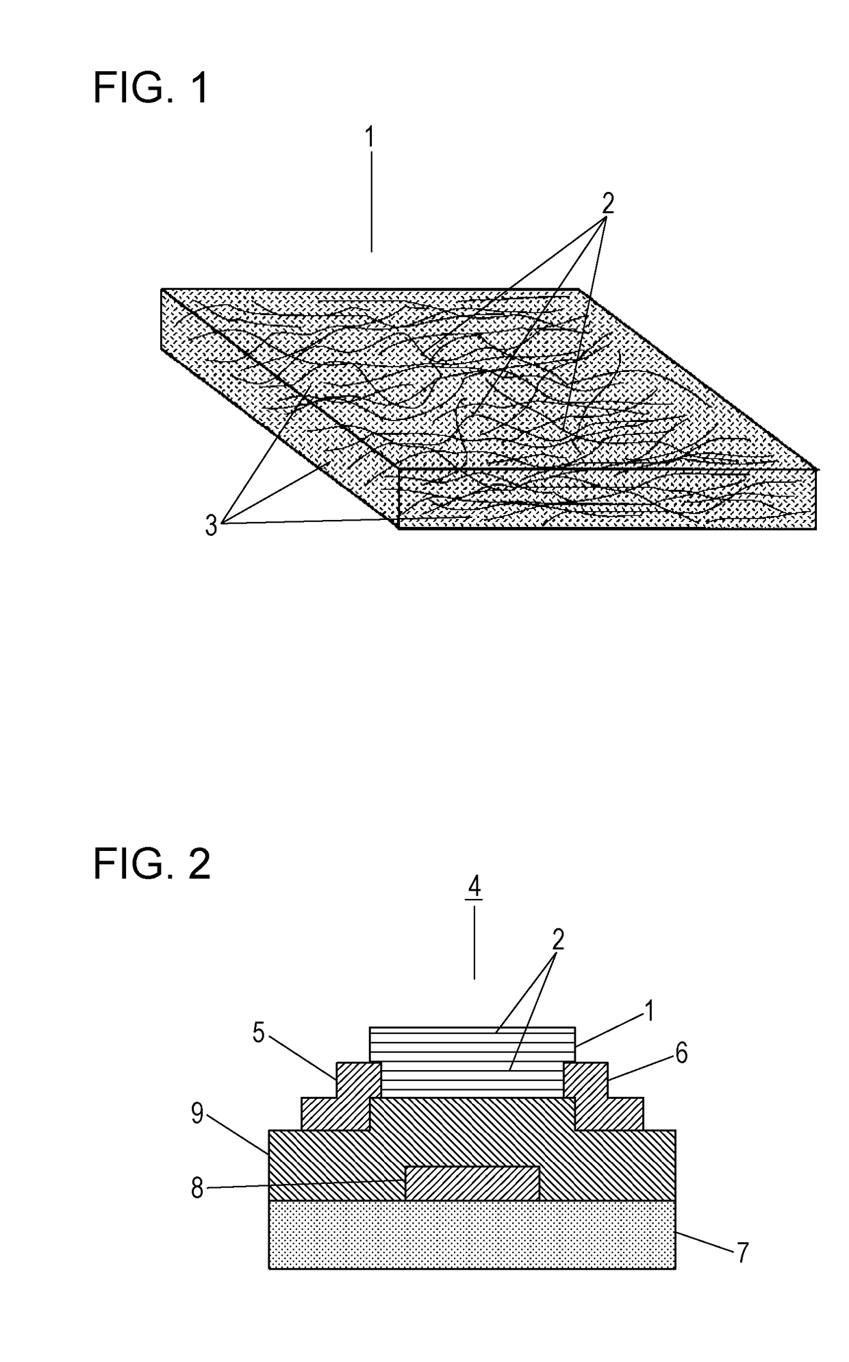
Phthalocyanine nanowires, ink composition and electronic element each containing same, and method for producing phthalocyanine nanowires
a technology of phthalocyanine nanowires and ink compositions, which is applied in the direction of non-metal conductors, applications, conductors, etc., can solve the problems of low solvent-solubility, difficulty in producing elements, and inability to meet the demand of general use of inorganic materials such as silicon, and achieve excellent semiconductor characteristics
- Summary
- Abstract
- Description
- Claims
- Application Information
AI Technical Summary
Benefits of technology
Problems solved by technology
Method used
Image

Examples
example 1
Production of Phthalocyanine Nanowire Ink Composition
[0172]First, 210 parts by mass of copper phthalocyanine sulfonyl chloride (degree of sulfonation=1) was added to a mixture containing 692 parts by mass of Surfonamine B-200 (trade name) (primary amine-terminated poly(ethylene oxide / propylene oxide) (5 / 95) copolymer, number-average molecular weight: about 2,000) manufactured by Huntsman Corporation as a polyether monoamine, 66 parts by mass of sodium carbonate, and 150 parts by mass of water, followed by reaction at 5° C. to room temperature for 6 hours. The resultant reaction mixture was heated to 90° C. under vacuum to remove water, thereby producing a copper phthalocyanine sulfamoyl compound represented by [Chem. 20] below.
[0173]
[0174]In the compound, Q represents a hydrogen atom or a methyl group, propylene oxide / ethylene oxide=29 / 6 (molar ratio), and average of n=35.
[0175]Step (1) (Precipitation Step)
[0176]First, 1.0 g of copper phthalocyanine (Fastogen Blue 5380 E, manufactur...
example 2
Production of Phthalocyanine Nanowire Ink Composition
[0187]A copper phthalocyanine nanowire ink composition (2) was produced by the same method as in Example 1 except that 1.67 g of copper phthalocyanine and 0.83 g of a phthalocyanine derivative of [Chem. 5] in place of [Chem. 20] in Example 1 were used. As a result of observation of phthalocyanine nanowires in the resultant phthalocyanine nanowire ink composition with a transmission electron microscope, it was confirmed that the nanowires have the shape of nanowires grown to a minor diameter of about 10 nm and a ratio of length to minor diameter of 50 or more (refer to FIGS. 7 and 8). Further, it was confirmed that the resultant phthalocyanine nanowires have high crystallinity characteristic of a phthalocyanine compound. In addition, the dispersion was extremely stable, and sedimentation of the phthalocyanine nanowires was not observed.
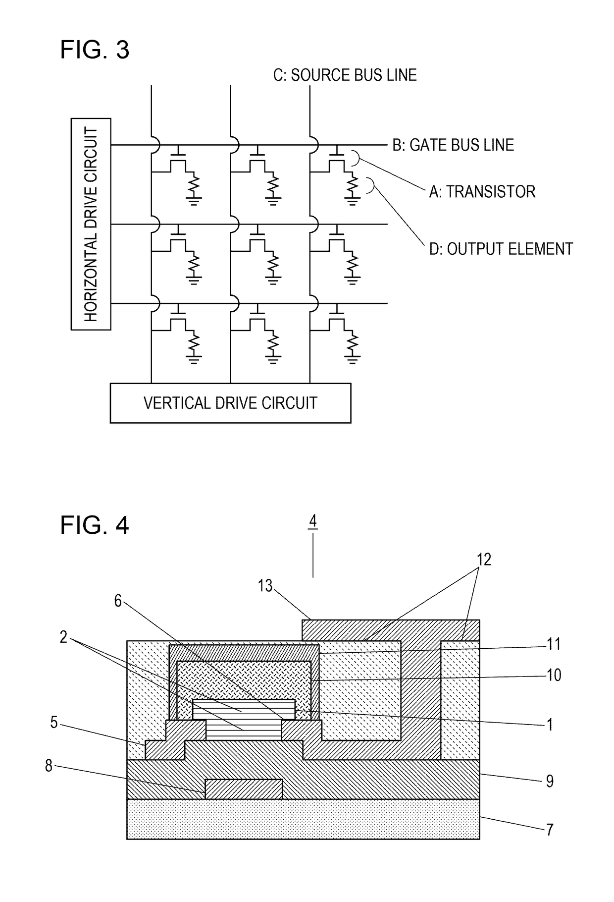
[0188]An organic transistor (2) was produced by the same method as in Example 1 except that the p...
example 3
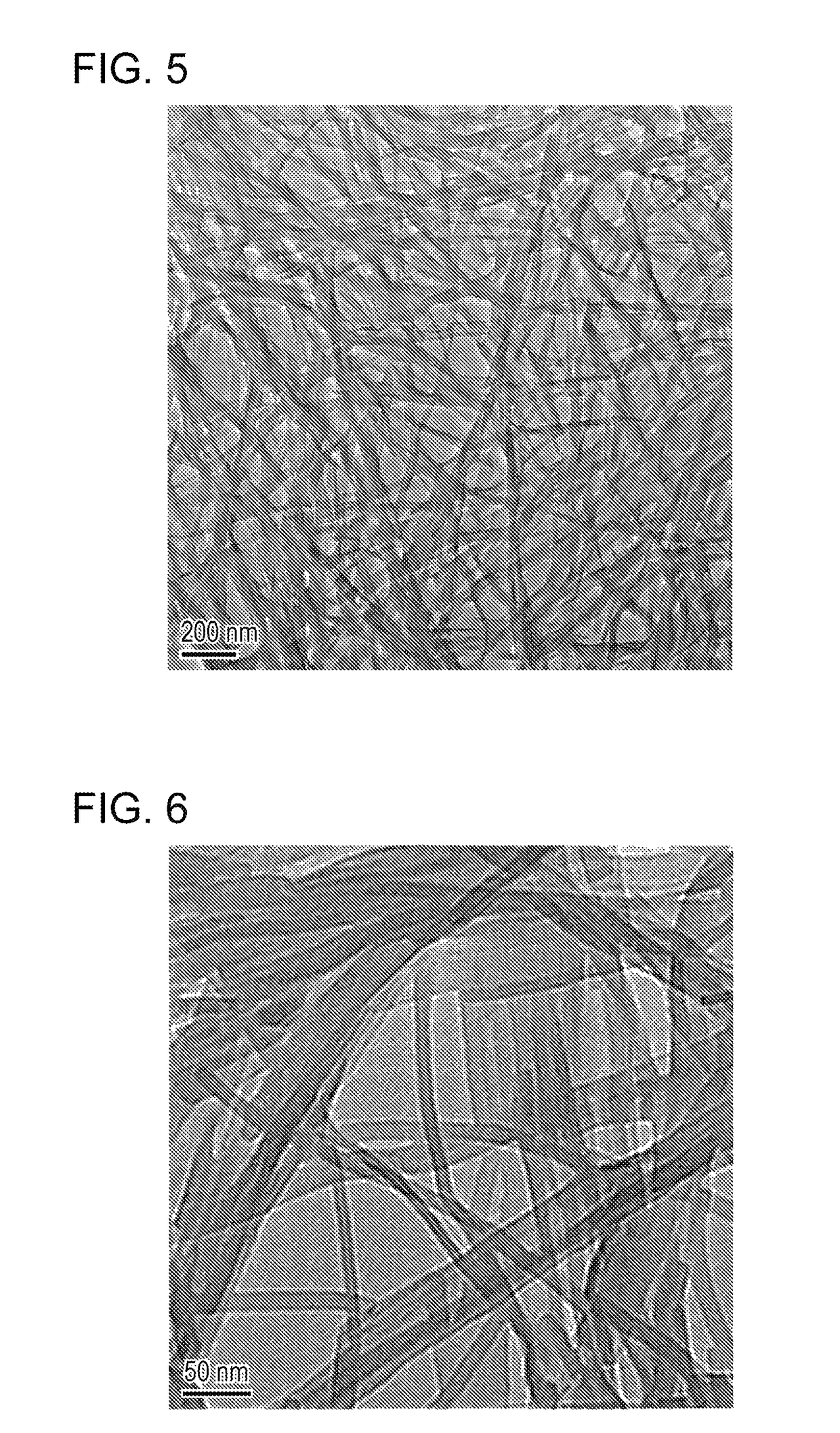
[0189]Copper phthalocyanine nanowires were produced by the same method as in Example 1 except that 1.67 g of copper phthalocyanine and 0.83 g of a phthalocyanine derivative of [Chem. 6] in place of [Chem. 20] in Example 1 were used. As a result of observation of the resultant phthalocyanine nanowire dispersion with a transmission electron microscope, it was confirmed that the nanowires have the shape of nanowires grown to a minor diameter of about 25 nm and a ratio of length to minor diameter of 10 or more (refer to FIGS. 9 and 10). Further, it was confirmed that the resultant phthalocyanine nanowires have high crystallinity characteristic of a phthalocyanine compound. In addition, the dispersion was extremely stable, and sedimentation of the phthalocyanine nanowires was not observed.
PUM
| Property | Measurement | Unit |
|---|---|---|
| length | aaaaa | aaaaa |
| diameter | aaaaa | aaaaa |
| particle diameter | aaaaa | aaaaa |
Abstract
Description
Claims
Application Information